Magnetoresistive head, magnetic storage apparatus and method of manufacturing a magnetic head
a technology of magnetic storage apparatus and magnetic head, which is applied in the direction of manufacturing tools, instruments, recording information storage, etc., can solve the problems of high frequency characteristics, difficult to enhance the sensitivity to the external field, and the disadvantage of tmr head for fast transfer, etc., and achieve high output
- Summary
- Abstract
- Description
- Claims
- Application Information
AI Technical Summary
Benefits of technology
Problems solved by technology
Method used
Image
Examples
embodiment 1
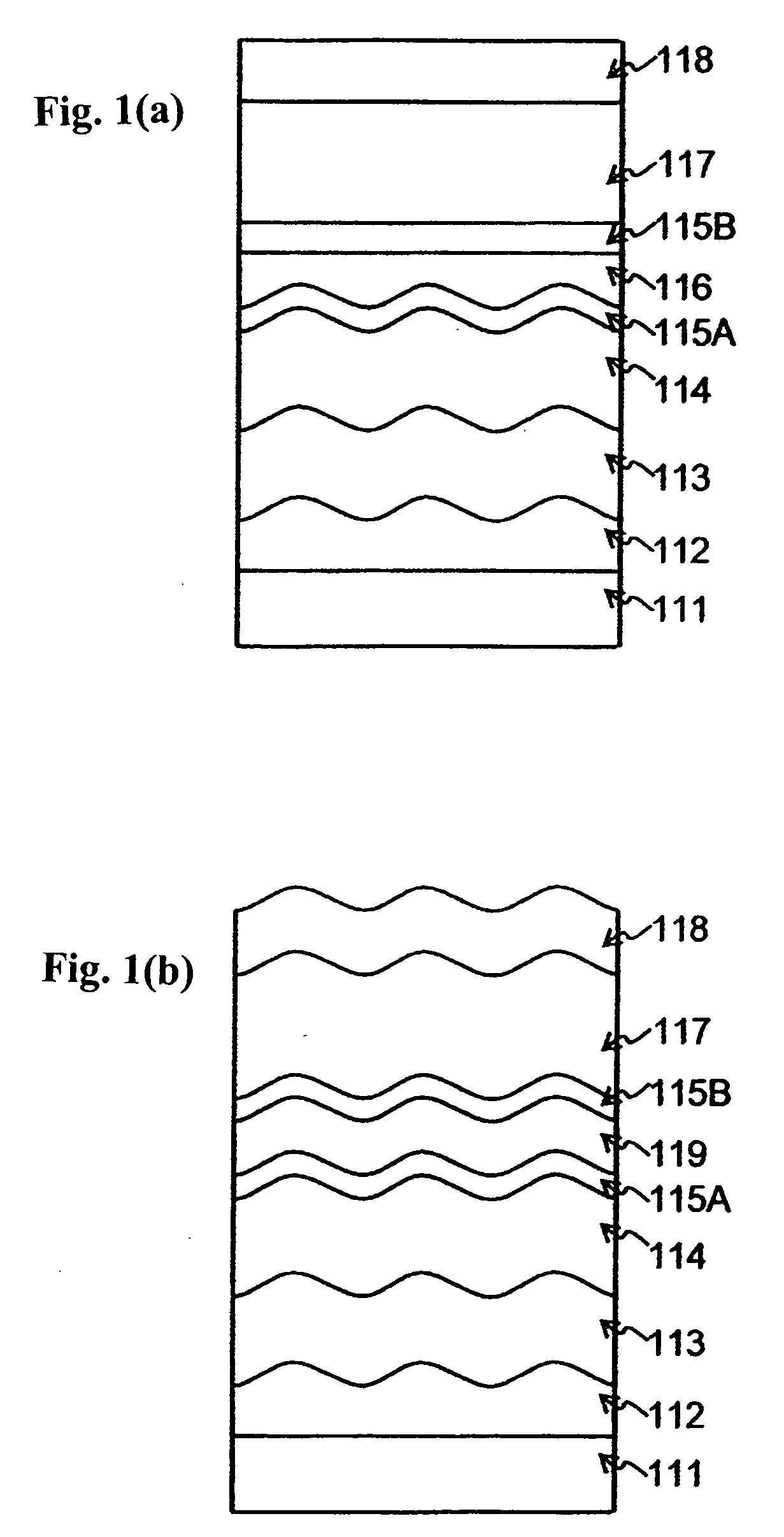
[0029]FIG. 1A is a cross-sectional schematic diagram showing a CPP-GMR device of a magnetic head according to Embodiment 1 of the present invention. More specifically, an NiFeCr film (5 nm) as an under layer 112, an MnIr film (6 nm) as an antiferromagnetic layer 113, and a CoFe (3 nm) / Ru (0.8 nm) / CoFe (3 nm) film of a synthetic ferri-magnetic structure as a ferromagnetic pinned layer 114 were formed over a substrate 111. The NiFeCr film used as the under layer was formed to enable the MnIr film (6 nm) of the antiferromagnetic layer to obtain high exchange coupling.
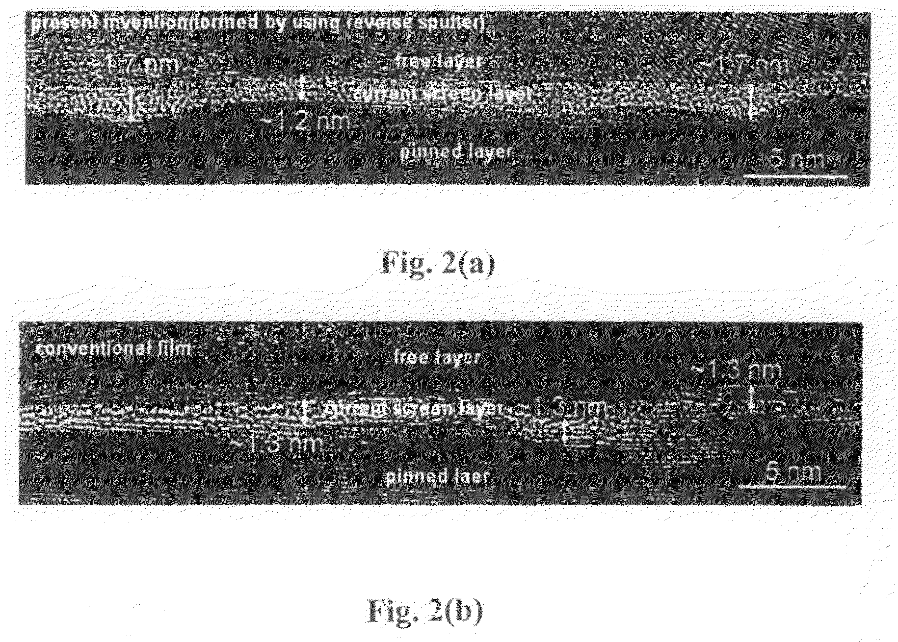
[0030]Then, after a Cu film (0.5 nm) as a non-magnetic intermediate layer 115A was formed, an Al90Cu10 film (subindices indicate at. %, and the same applies hereinafter) (1.0 nm) as a current screen layer 116 was formed, and subsequently, natural oxidation was applied thereto under a pressure at 500 Pa for one minute. The non-magnetic intermediate layer 115A functions as an anti-oxidizing layer for the pinned layer when th...
embodiment 2
[0042]There were prepared specimens of devices where a film thickness before oxidation with respect to the current screen layer 116 in the structure according to embodiments of the present invention, shown in FIG. 1A, and the current screen layer 119 in the conventional structure, shown in FIG. 1B, respectively, was varied in a range of from 0.86 to 1.6 nm. Other layers, and conditions of the reverse sputtering are the same as those for Embodiment 1. In this case, a difference in film thickness, tthick−tthin, between the thickest part of the current screen layer of the specimen of the device according to embodiments of the present invention, and the thinnest part tthin thereof was found constant regardless of the film thickness of the current screen layer, that is, tthick−tthin=0.4 nm.
[0043]In general, at the time of measurement on a magnetization curve of a spin-valve film, a magnetization curve shift Hint is observed against the axis at H=0 (Oe) in the magnetization curve of a fre...
embodiment 3
[0049]The current screen layer 116 in the structure according to embodiments of the present invention, shown in FIG. 1A, and the current screen layer 119 in the conventional structure shown in FIG. 1B were formed by sputtering in an atmosphere of mixture of argon flowing at 20 sccm, and oxygen flowing at 2 sccm. For a sputter target, use was made of Al90Cu10. There were prepared specimens of devices where a film thickness of the current screen layer, after oxidation, was varied in a range of from 0.5 to 2.0 nm. Other layers, and conditions of the reverse sputtering are the same as those for Embodiment 1. In this case, a difference in film thickness, tthick−tthin, between the thickest part of the current screen layer 116 of the specimen of the device according to embodiments of the present invention, and the thinnest part tthin thereof was found constant at tthick−tthin=0.4 nm regardless of the film thickness of the current screen layer.
[0050]FIG. 8 shows a relationship between a mag...
PUM
| Property | Measurement | Unit |
|---|---|---|
| pressure | aaaaa | aaaaa |
| surface roughness | aaaaa | aaaaa |
| surface roughness | aaaaa | aaaaa |
Abstract
Description
Claims
Application Information
 - R&D
- Intellectual Property
- Life Sciences
- Materials
- Tech Scout
- Unparalleled Data Quality
- Higher Quality Content
- 60% Fewer Hallucinations
Browse by: Latest US Patents, China's latest patents, Technical Efficacy Thesaurus, Application Domain, Technology Topic, Popular Technical Reports.
© 2025 PatSnap. All rights reserved.Legal|Privacy policy|Modern Slavery Act Transparency Statement|Sitemap|About US| Contact US: help@patsnap.com


