Non-volatile memory and manufacturing method and erasing method thereof

a manufacturing method and non-volatile memory technology, applied in the field of memory devices, can solve the problems of low relatively high production cost, and erasing time of the conventional single poly non-volatile memory, and achieve the effects of reducing erasing time, increasing cycling number, and accelerating the operating speed of the memory devi

Inactive Publication Date: 2008-05-01
EPISIL TECH INC
View PDF5 Cites 4 Cited by
  • Summary
  • Abstract
  • Description
  • Claims
  • Application Information

AI Technical Summary

Benefits of technology

[0009]Accordingly, the present invention is directed to provide a non-volatile memory and a manufacturing method and an erasing method thereof, which are capable of reducing the erasing time, accelerating the operating speed of the device, and increasing the cycling numbers.
[0024]In the non-volatile memory of the invention, since the heavily doped region formed in the substrate is used as the control gate, and an erase gate is formed above the floating gate, the chip size is not increased. Hence, the manufacturing cost will not be increased and the integration of the device will not be compromised. Additionally, in the erasing operation of the non-volatile memory of this invention, because a high voltage is applied on the erase gate for drawing the electrons to the erase gate to be erased, the non-volatile memory of this invention will not suffer the problem of damages in the gate oxide layer as the conventional single poly non-volatile memory, and the cycling number and the reliability of the memory device can be improved. Furthermore, the non-volatile memory of this invention affords shorter operating time for the erasing operation. In addition, because the top edge of the floating gate is sharp-angled, the erasing speed is further accelerated during the erasing operation.

Problems solved by technology

However, the conventional single poly non-volatile memory encounters a few problems.
For example, the conventional single poly non-volatile memory including the NMOS structure 10 and the PMOS structure 12 occupies a much larger chip area, which results in a relatively high production cost.
On the other hand, the conventional single poly non-volatile memory takes a longer time to erase data, resulting in low operating speed of the memory device.
Moreover, for the erasing operation of the conventional single poly non-volatile memory, the electrons are drawn from the floating gate to the substrate through the gate oxide layer, and the gate oxide layer may be easily damaged, thus adversely affecting the cycling number and the reliability of the memory device.
However, the memory device employing the conventional split gate non-volatile memory has a larger size, and electron can be trapped easily for the erasing operation, thus lowering endurance of the memory device.

Method used


Image

  • Non-volatile memory and manufacturing method and erasing method thereof
  • Non-volatile memory and manufacturing method and erasing method thereof
  • Non-volatile memory and manufacturing method and erasing method thereof

Examples


Embodiment Construction

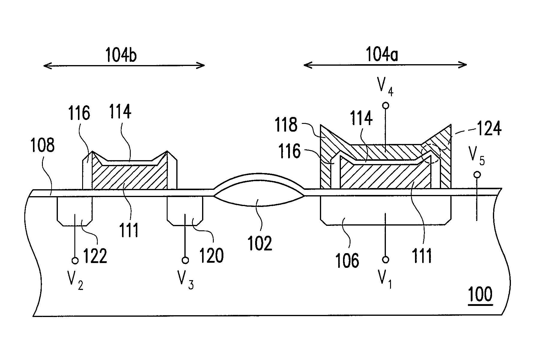
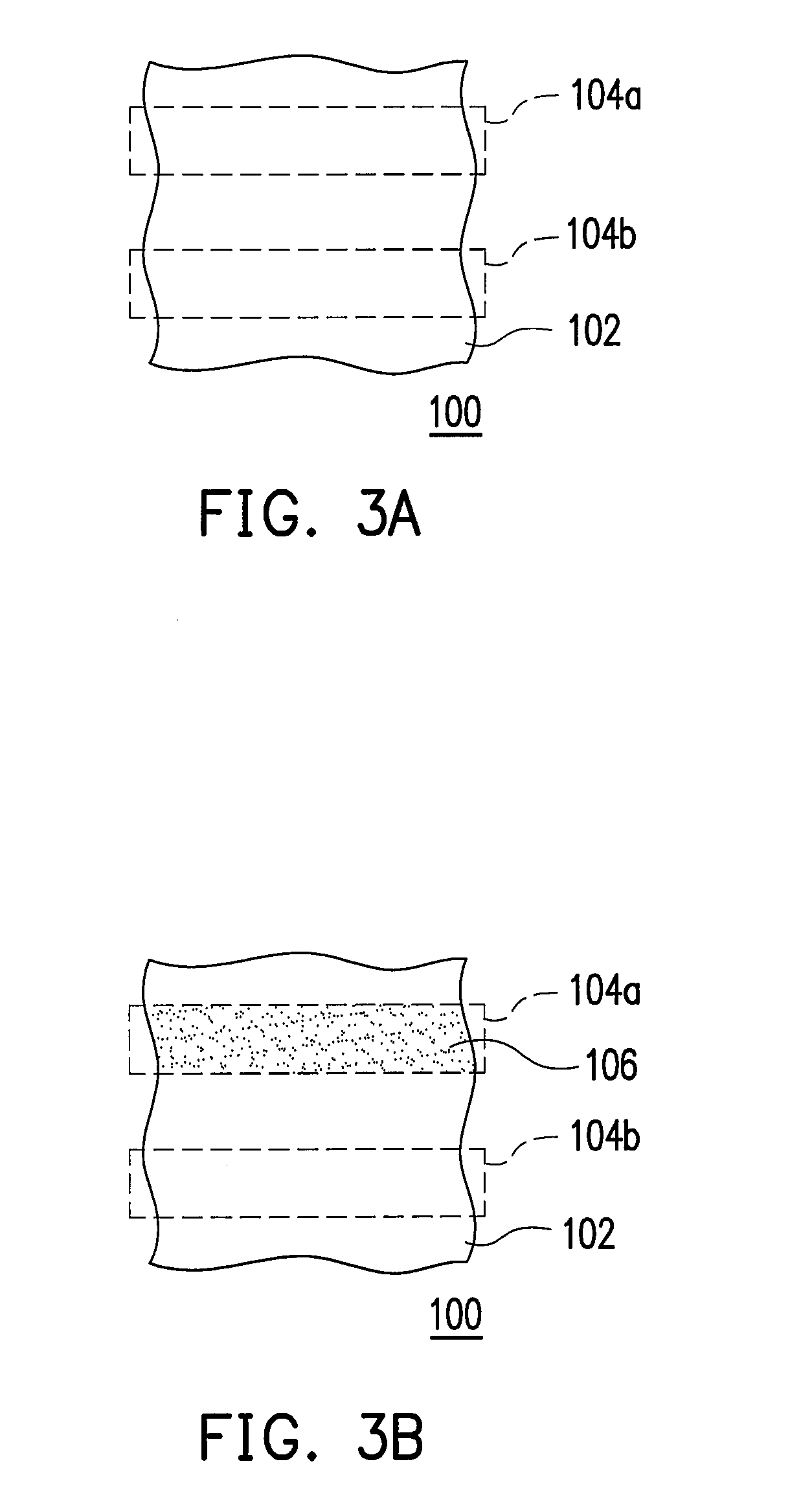
[0032]FIGS. 3A-3H are top views of the steps of the manufacturing method of the non-volatile memory according to one embodiment of the invention.

[0033]Firstly, with reference to FIG. 3A, a device isolation structure 102 is formed in a substrate 100 for defining a pair of active regions 104a and 104b. The device isolation structure 102 is, for example, a field oxide layer, and the method for forming the same is, for example, local oxidation of silicon (LOCOS).

[0034]Then, with reference to FIG. 3B, a control gate 106 is formed in one of the active regions 104a and 104b of the substrate 100. In the embodiment, forming the control gate 106 in the active region 104a of the substrate 100 is taken as an example. The control gate 106 is, for example, a heavily doped region formed in the substrate 100, formed by ion-implantation.

[0035]Subsequently, with reference to FIG. 3C, a gate oxide layer 108, a conductor layer 110, and a patterned mask layer 112 are formed on the substrate 100 in seque...


PUM


Abstract

A non-volatile memory is provided, including a control gate, a floating gate, a gate oxide layer, a source region, a drain region, a first dielectric layer, a second dielectric layer, and an erase gate. The control gate is disposed in a substrate. The floating gate comprising a coupling part and a gate part is disposed over the control gate and located over a portion of the substrate with the gate oxide layer there-between. The source region adjoins with one side of the gate part, while the drain region adjoins with the other side of the gate part. The first dielectric layer is disposed on the floating gate. The second dielectric layer is disposed on the sidewalls of the floating gate. The erase gate is disposed over the coupling part of the floating gate and covers the first dielectric layer and the second dielectric layer.

Description

BACKGROUND OF THE INVENTION[0001]1. Field of Invention[0002]The present invention relates to a memory device. More particularly, the present invention relates to a non-volatile memory and a manufacturing method and an erasing method thereof.[0003]2. Description of Related Art[0004]Memory, just as its name implies, is a semiconductor device for storing information and data. Memory is required to perform more and more effectively as the functions of microprocessors become stronger and the programs and calculations of software become larger. Memory with mass storage and low cost must be manufactured to meet the requirements of this trend. Therefore, the process of manufacturing such memory devices continuously develops for the semiconductor technology with higher integration.[0005]Among memories, non-volatile memory is capable of storing, reading, or erasing data repeatedly, and the stored data will not disappear after the power supply is disconnected. Because of these advantages, non-...

Claims


Application Information

Patent Timeline
Patent Type & Authority Applications(United States)
IPC IPC(8): H01L29/788H01L21/8238
CPCH01L27/115H01L27/11519H01L29/42324H01L27/11558H01L27/11521
Inventor HUNG, CHIH-LUNG
Owner EPISIL TECH INC
Why Eureka
Try Eureka