Display substrate and method of manufacturing a motherboard for the same

a technology of a substrate and a manufacturing method, which is applied in the direction of static indicating devices, semiconductor/solid-state device testing/measurement, instruments, etc., can solve the problems of short circuit between conductors or switching elements, conductor lines exposed, and pollutant generation, so as to improve product reliability and simplify manufacturing processes

Active Publication Date: 2008-03-27
TCL CHINA STAR OPTOELECTRONICS TECH CO LTD
View PDF8 Cites 41 Cited by
  • Summary
  • Abstract
  • Description
  • Claims
  • Application Information

AI Technical Summary

Benefits of technology

[0010]According to the display substrate and the method of manufacturing the motherboard for the display substrate, the first electrostatic dispersion lines may connect the test pad electrode of the test pad to the electrical shorting bar so that the electrical shorting bar may disperse the electric charges inflowing from the test pad into a large area to prevent static electricity from being generated. Therefore, the motherboard for the display substrate may be prevented from being damaged by the static electricity so that the reliability of products may be improved and manufacturing processes may be simplified.

Problems solved by technology

In the diamond cutting method, a pollutant may be generated during the diamond cutting process and conductor lines exposed due to cutting may corrode.
During the manufacture of the liquid crystal display apparatus, static electricity may be may be present and may cause a short circuit between conductors or switching elements.
Various methods and devices have been proposed to prevent static electricity but additional manufacturing costs and processes may be incurred.

Method used


Image

  • Display substrate and method of manufacturing a motherboard for the same
  • Display substrate and method of manufacturing a motherboard for the same
  • Display substrate and method of manufacturing a motherboard for the same

Examples


Embodiment Construction

[0018]The invention is described more fully hereinafter with reference to the accompanying drawings, in which embodiments of the invention are shown. This invention may, however, be embodied in many different forms and should not be construed as limited to the embodiments set forth herein.

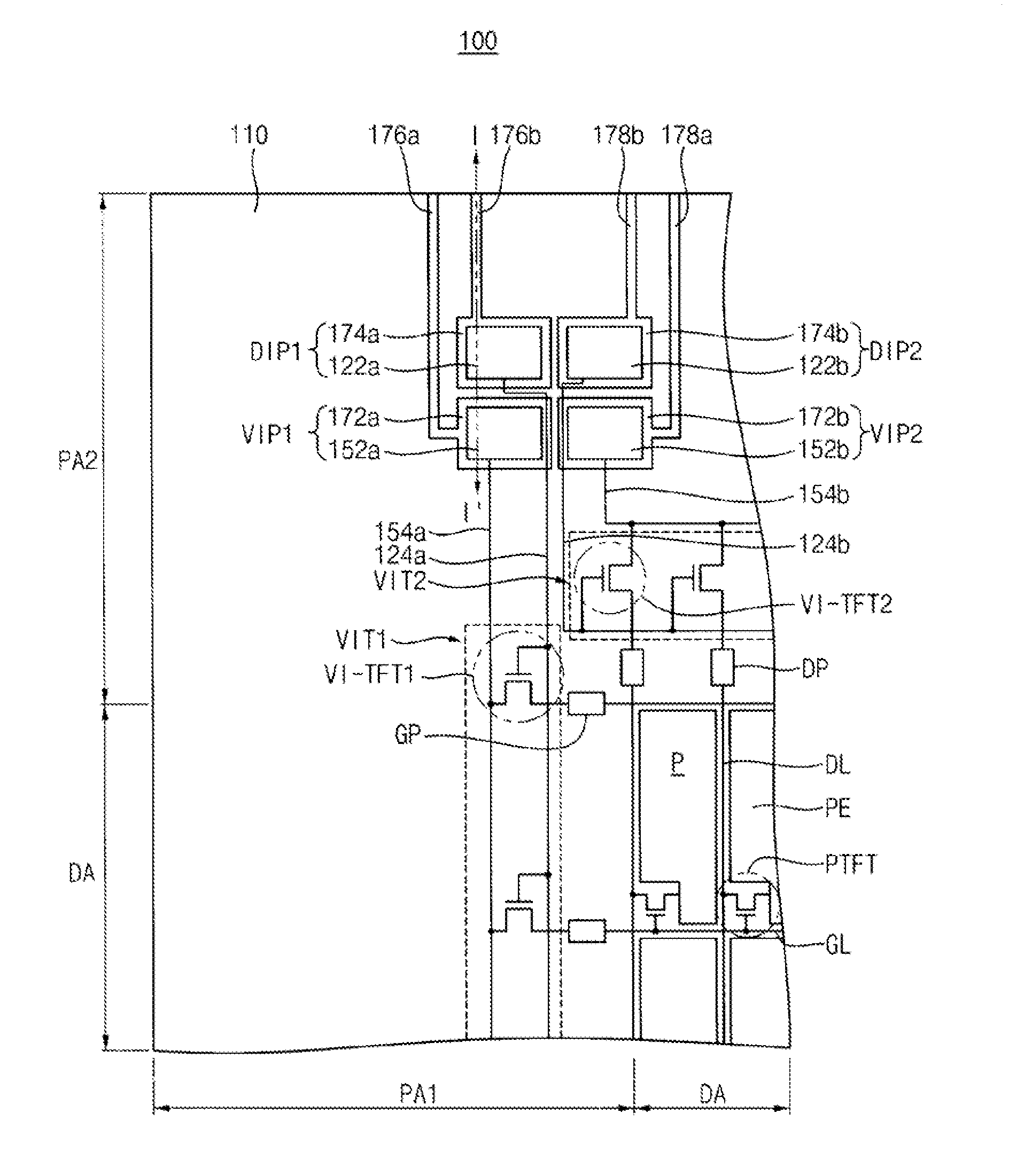
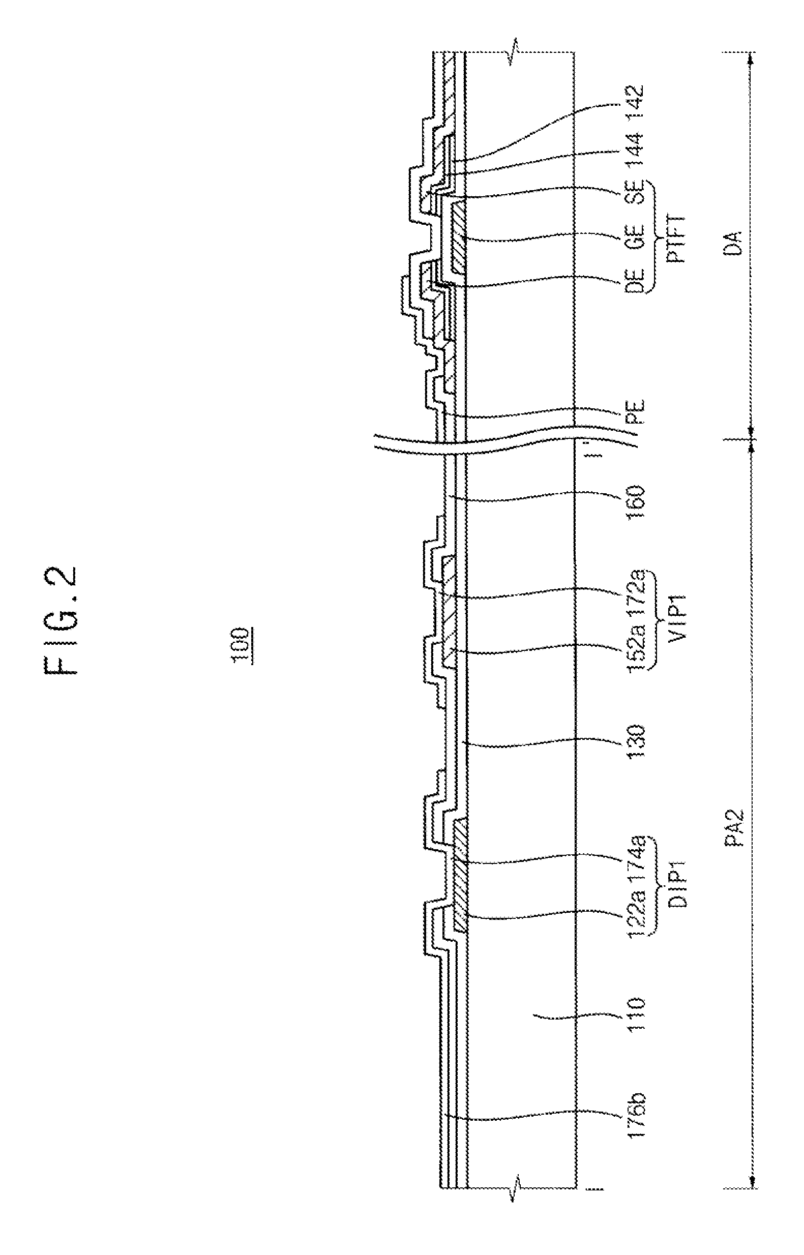
[0019]FIG. 1 is a plan view illustrating a display substrate according to an exemplary embodiment of the present invention. FIG. 2 is a cross-sectional view taken along a line I-I′ shown in FIG. 1.

[0020]Referring to FIGS. 1 and 2, a display substrate 100 according to an exemplary embodiment of the present invention includes a base substrate 110. The base substrate 110 includes a display area DA, a first peripheral area PA1 and a second peripheral area PA2. The display area DA includes a plurality of in pixel areas P. The first and second peripheral areas PA1 and PA2 surround the display area DA.

[0021]A gate line GL, a data line DL, a pixel switching element PTFT and a pixel electrode are formed in ...


PUM


Abstract

A display substrate includes a signal line, a test switch, a test pad, and a first electrostatic dispersion line. The signal line is formed in the display area of a base substrate. The test switch is formed in a peripheral area of the base substrate surrounding the display area. The test switch applies a test signal to the signal line. The test pad is electrically connected to the test switch and receives the test signal The first electrostatic dispersion line is extended from the test pad to an end of the base substrate.

Description

CROSS-REFERENCE TO RELATED APPLICATION[0001]This application claims priority under 35 U.S.C. §119 to Korean Patent Application No. 2006-92034, filed on Sep. 22, 2006, and No. 2007-38660, filed on Apr. 20, 2007, in the Korean Intellectual Property Office (KIPO), the contents of which are herein incorporated by reference in their entirety.BACKGROUND OF THE INVENTION[0002]1. Technical Field[0003]The present invention relates to a display substrate and a method of manufacturing a motherboard for the display substrate.[0004]2. Discussion of the Related Art[0005]As part of a process in the manufacture of a liquid crystal display, a visual inspection (VI) or a gross test (GT) is performed before integrated circuits are mounted on a liquid crystal display panel. The VI or the GT inspects a pixel voltage applied to a pixel electrode of an array substrate. The VI or the GT inspects errors before a process of manufacturing the liquid crystal display panel is completed so that manufacturing cos...

Claims


Application Information

Patent Timeline
Patent Type & Authority Applications(United States)
IPC IPC(8): G01R31/00H01L21/02
CPCG02F1/13458G02F1/136204G09G3/3648G09G3/006G02F2001/136254G02F1/136254
Inventor KIM, HYUN-YOUNGYOU, CHUN-GILEE, JAE-BOKJUNG, KWAN-WOOKNA, HYUNG-DONTAE, SEUNG-GYUKIM, JUNG-YUN
Owner TCL CHINA STAR OPTOELECTRONICS TECH CO LTD
Why Eureka
Try Eureka