NROM fabrication method
a technology of nitride and read only memory, which is applied in the direction of semiconductor devices, electrical devices, transistors, etc., can solve the problems of limiting the extent to which the cell size can be shrunk, the planarized oxide is not a clean oxide nor does it seal, and the process is complicated and expensiv
- Summary
- Abstract
- Description
- Claims
- Application Information
AI Technical Summary
Benefits of technology
Problems solved by technology
Method used
Image
Examples
first embodiment
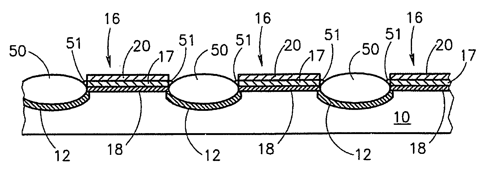
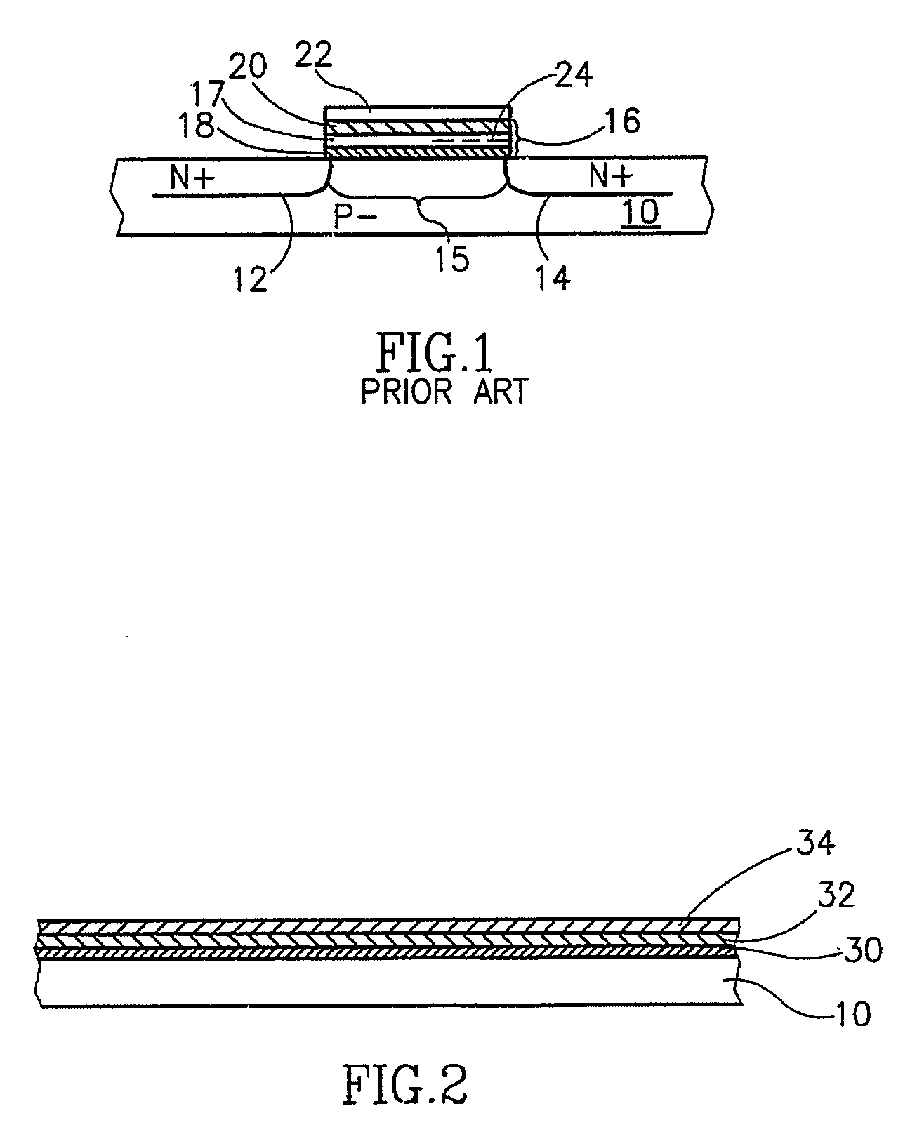
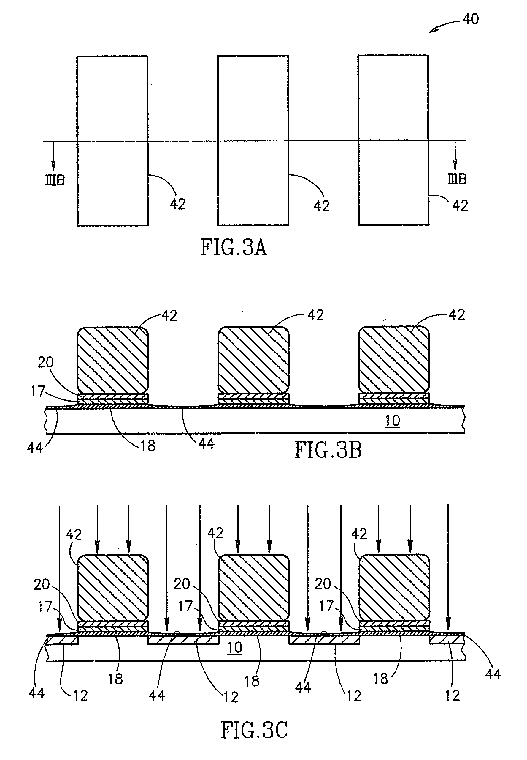
[0052]Specifically, in the first embodiment, after mask 52 is laid down, the threshold voltage level adjustment is performed. This procedure involves implanting boron through the ONO layers into the portions of the periphery of the chip not covered by mask 52. Typically, there are two adjustment steps, one each for the n-channel and p-channel transistors. It will be appreciated that, in accordance with a preferred embodiment of the present invention, the adjustment implant is performed though the ONO layers since they are not yet capped and thus, do not block the implant operation. It will further be appreciated that, for the threshold adjustment procedure, the to-be-removed ONO layers act as a sacrificial oxide (e.g. an oxide grown for an implant operation and immediately thereafter removed).
[0053]Following the threshold voltage adjustment procedure, the ONO layers on the unmasked portions of the chip are removed. Initially, a dry oxide etch is utilized to remove top oxide 34 and n...
second embodiment
[0055]In a second embodiment, mask 52 is laid down after the gate and threshold voltage level adjustment procedure is performed. Thus, the memory array portion of the chip also receives threshold level adjustments. With mask 52 in place, the ONO layers on the unmasked portions of the chip are removed, as described hereinabove. Once again, the ONO layers act as a sacrificial oxide, eliminating the necessity for the additional sacrificial oxide operations.
[0056]Finally, following removal of mask 52, a gate oxide is grown over the entire array, creating gate oxides in the periphery only.
[0057]Following the gate oxide growth step, a polysilicon layer, which will create word lines for the memory array portion and will create gates for the periphery transistors, is laid down over the chip. If desired, a low resistive silicide, as is known in the art, can be deposited over the polysilicon layer in order to reduce its resistivity. This creates a “polysilicide” layer. A typical total thickne...
PUM
| Property | Measurement | Unit |
|---|---|---|
| thickness | aaaaa | aaaaa |
| thickness | aaaaa | aaaaa |
| temperature | aaaaa | aaaaa |
Abstract
Description
Claims
Application Information
 - R&D
- Intellectual Property
- Life Sciences
- Materials
- Tech Scout
- Unparalleled Data Quality
- Higher Quality Content
- 60% Fewer Hallucinations
Browse by: Latest US Patents, China's latest patents, Technical Efficacy Thesaurus, Application Domain, Technology Topic, Popular Technical Reports.
© 2025 PatSnap. All rights reserved.Legal|Privacy policy|Modern Slavery Act Transparency Statement|Sitemap|About US| Contact US: help@patsnap.com


