Layered Thin Film Structure, Layered Thin Film Forming Method, Film Forming System and Storage Medium

a technology of layered film and forming method, which is applied in the direction of layered products, transportation and packaging, coatings, etc., can solve the problems of inability to control the content of alloying elements of copper alloy films, the inability to fill up recesses in the surface of wafers satisfactorily, and the inability to form films by sputtering processes. achieve satisfactory step coverage and high adhesion

Inactive Publication Date: 2008-03-20
TOKYO ELECTRON LTD
View PDF6 Cites 1 Cited by
  • Summary
  • Abstract
  • Description
  • Claims
  • Application Information

AI Technical Summary

Benefits of technology

[0026] The layered thin film structure, the layered thin film structure forming method of forming the same, the film forming system and the storage medium according to the present invention exercise the following effects.
[0027] Since the alloy layer is formed by executing at least one cycle of the alternate steps of forming the alloying-element film of the first metal as the alloying metal and forming the base-metal film of the second metal, the alloy layer can be bonded to the underlying layer by high adhesion, the peeling of the alloy layer off the underlying layer can be suppressed, satisfactory step coverage can be achieved even under high miniaturization, and the alloying element can be satisfactorily diffused.

Problems solved by technology

Although the copper alloy film is formed by a sputtering process, the formation of a film by a sputtering process has difficulty in satisfying step coverage required by current design rules specifying fine wiring lines and cannot satisfactorily filling up recesses in the surface of a wafer.
Therefore, it has been impossible to control the alloying element content of a copper alloy film such that specific parts of the copper alloy film have, for example, a high alloying element content.
Therefore, migration cannot be satisfactorily suppressed.
Consequently, the copper alloy film and the underlying layer could not have been bonded together by sufficiently high adhesion and, in some cases, peeling off of the copper alloy film from the underlying layer could not have been prevented.
However, a CVD process can form only a metal film of a single kind at a time and a simple application of a CVD process cannot evenly mix or disperse atoms of an alloying element in a film.

Method used


Image

  • Layered Thin Film Structure, Layered Thin Film Forming Method, Film Forming System and Storage Medium
  • Layered Thin Film Structure, Layered Thin Film Forming Method, Film Forming System and Storage Medium
  • Layered Thin Film Structure, Layered Thin Film Forming Method, Film Forming System and Storage Medium

Examples


Embodiment Construction

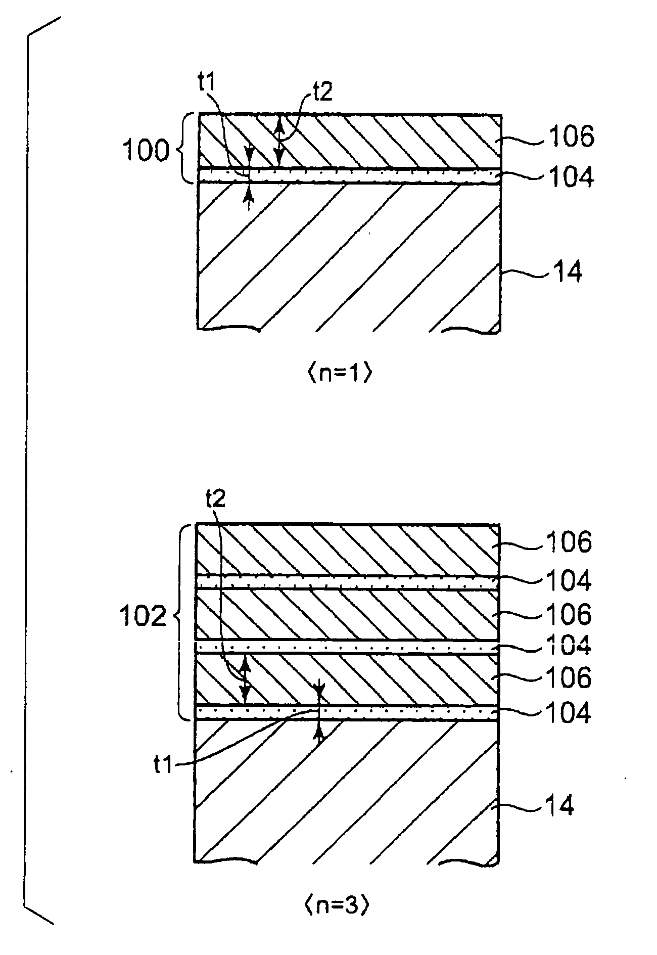
[0034] A layered thin film structure, a layered thin film structure forming method of forming the same, a film forming system and a storage medium in preferred embodiments according to the present invention will be described with reference to the accompanying drawings.

[0035]FIG. 1 is a block diagram of a film forming system in a preferred embodiment according to the present invention.

[0036] The film forming system of the present invention will be described. The film forming system 2 has a cylindrical processing vessel 4 of, for example, aluminum. The processing vessel 4 is grounded. The processing vessel 4 has a bottom wall provided with an exhaust port 6. An evacuating system 12 including a pressure regulating valve 8 and a vacuum pump 10 is connected to the exhaust port 6. The evacuating system 12 evacuates the processing vessel 4 at a desired pressure.

[0037] A gate valve 16 is attached to the side wall of the processing vessel 4. The gate valve 16 is opened to carry a semicond...


PUM

PropertyMeasurementUnit
frequencyaaaaaaaaaa
temperatureaaaaaaaaaa

Abstract

There is provided a layered thin film structure forming method capable of forming a layered thin film structure bonded to an underlying layer by high adhesion, of suppressing the peeling of the layered thin film structure off the underlying layer, of achieving satisfactory step coverage even under high miniaturization, and of satisfactorily diffusing an alloying element. A layered thin film structure forming method of forming a layered thin film structure by depositing a plurality of thin films on a surface of a workpiece in a processing vessel capable of being evacuated includes the steps of: forming an alloying-element film 104 of a first metal by using a source gas containing the first metal as an alloying element, and a reducing gas; and forming a base-metal film 106 of a second metal in a thickness greater than that of the alloying-element film by using a source gas containing the second metal, and a reducing gas. At least one cycle of the alternate steps of forming the alloying-element film and forming the base-metal film is executed.

Description

TECHNICAL FIELD [0001] The present invention relates to a layered thin film structure to be formed on a surface of a substrate, such as a semiconductor wafer, a layered thin film structure forming method of forming the same, a film forming system for carrying out the layered thin film structure forming method, and a storage medium storing a program for controlling the film forming system. BACKGROUND ART [0002] Generally, a workpiece, such as a semiconductor wafer, is subjected repeatedly to processes including a film forming process, an etching process, an oxidation and diffusion process, an annealing process and a modification process to form a semiconductor integrated circuit, such as an IC or a LSI, on the substrate. Thickness of wiring layers and the width of lines have been progressively reduced to meet demand for further increasing the scale of integration, further device miniaturization and further increase in operating speed. Use of copper wiring lines having low resistance ...

Claims


Application Information

Patent Timeline
Patent Type & Authority Applications(United States)
IPC IPC(8): H01L21/44B32B7/02C23C16/00
CPCC23C16/06C23C16/45529Y10T428/24975Y10T428/2495C23C16/45542C23C16/45553C23C16/52
Inventor YOSHII, NAOKIKOJIMA, YASUHIKOSATO, HIROSHI
Owner TOKYO ELECTRON LTD
Why Eureka
Try Eureka