Diffusing agent composition and method of manufacturing semiconductor substrate

a technology of diffusing agent and composition, which is applied in the direction of other chemical processes, coatings, chemistry apparatus and processes, etc., can solve the problems of reducing and difficult to uniformly implant ions, so as to reduce the performance of the element

Active Publication Date: 2019-03-26
TOKYO OHKA KOGYO CO LTD
View PDF6 Cites 0 Cited by
  • Summary
  • Abstract
  • Description
  • Claims
  • Application Information

AI Technical Summary

Benefits of technology

[0010]In the semiconductor substrate which includes, on its surface, a three-dimensional structure on a nanometer scale, in order to enhance the uniformity of the diffusion of an impurity diffusion component, a coating-type diffusing agent composition is considered to be used. In the substrate which includes, on its surface, a three-dimensional structure having small air gaps on a nanometer scale, all surfaces including the entire inner surface of the small air gaps can be uniformly coated with the coating-type diffusing agent composition, and thus in the semiconductor substrate having a three-dimensional surface, an impurity such as boron can be uniformly diffused.
[0012]In the coating-type diffusing agent composition, even when the time of the cycle of heating and cooling is shortened or heating at a low temperature is performed, it is preferable that an impurity can be satisfactorily diffused. Although it is further necessary to control the length of diffusion as a result of realization of three-dimensional structures, it is considered that diffusion is performed by heating at a low temperature and that thus it is possible to shorten the length of diffusion.
[0013]The present invention is made in view of the foregoing problems, and an object thereof is to provide: a diffusing agent composition where even when a semiconductor substrate into which an impurity diffusion component is diffused includes, on its surface, a three-dimensional structure having, on its surface, small air gaps on a nanometer scale, on the surfaces of the semiconductor substrate including the entire inner surface of the small air gaps, a coating film can be formed whose film thickness is uniform and which is homogeneous without tarnishing, and where thus even when heating is performed, for example, at a low temperature equal to or less than 1000° C., it is possible to satisfactorily and uniformly diffuse boron into the semiconductor substrate; and a method of manufacturing a semiconductor substrate using the diffusing agent composition described above.
[0026]According to the present invention, it is possible to provide: a diffusing agent composition where even when a semiconductor substrate into which an impurity diffusion component is diffused includes, on its surface, a three-dimensional structure having, on its surface, small air gaps on a nanometer scale, on the surfaces of the semiconductor substrate including the entire inner surface of the small air gaps, a coating film can be formed whose film thickness is uniform and which is homogeneous without tarnishing, and where thus even when heating is performed, for example, at a low temperature equal to or less than 1000° C., it is possible to satisfactorily and uniformly diffuse boron into the semiconductor substrate; and a method of manufacturing a semiconductor substrate using the diffusing agent composition described above.

Problems solved by technology

However, in the ion implantation method as disclosed in Patent Document 1, when a light ion such as B (boron) is implanted into the semiconductor substrate, in a region near the surface of the substrate, a point defect or a point defect cluster is easily formed.
For example, when an impurity diffusion component is diffused by the ion implantation method into a semiconductor substrate, and thus an element such as a CMOS image sensor is formed, the occurrence of such a defect directly leads to a reduction in the performance of the element.
For example, when a semiconductor substrate includes, on its surface, a three-dimensional structure on a nanometer scale such as a three-dimensional structure for forming a multi-gate element called a Fin-FET which includes a plurality of source fins, a plurality of drain fins and gates orthogonal to those fins, in the ion implantation method, it is difficult to uniformly implant ions into the side surface and the upper surface of the fins and gates and the entire inner surface of a concave portion surrounded by the fins and the gates.
When an impurity diffusion component is diffused by the ion implantation method into a semiconductor substrate having a three-dimensional structure on a nanometer scale, even if the uniform implantation of ions is achieved, there are failures which will be described below.
For example, when a semiconductor substrate which includes a three-dimensional pattern having small fins is used so as to form a logic LSI device or the like, the crystal of a substrate material such as silicon is easily damaged by ion plantation.
It is considered that the damaged crystal causes a failure such as a variation in the property of the device or the production of a standby leak current.

Method used


Image

  • Diffusing agent composition and method of manufacturing semiconductor substrate
  • Diffusing agent composition and method of manufacturing semiconductor substrate
  • Diffusing agent composition and method of manufacturing semiconductor substrate

Examples


examples

[0110]Although the present invention will be more specifically described below using examples, the present invention is not limited to the examples below.

examples 1 to 22

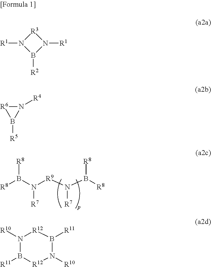
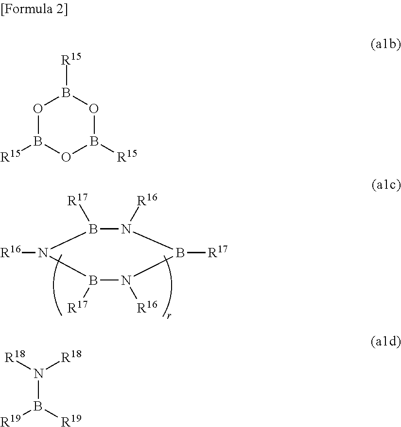
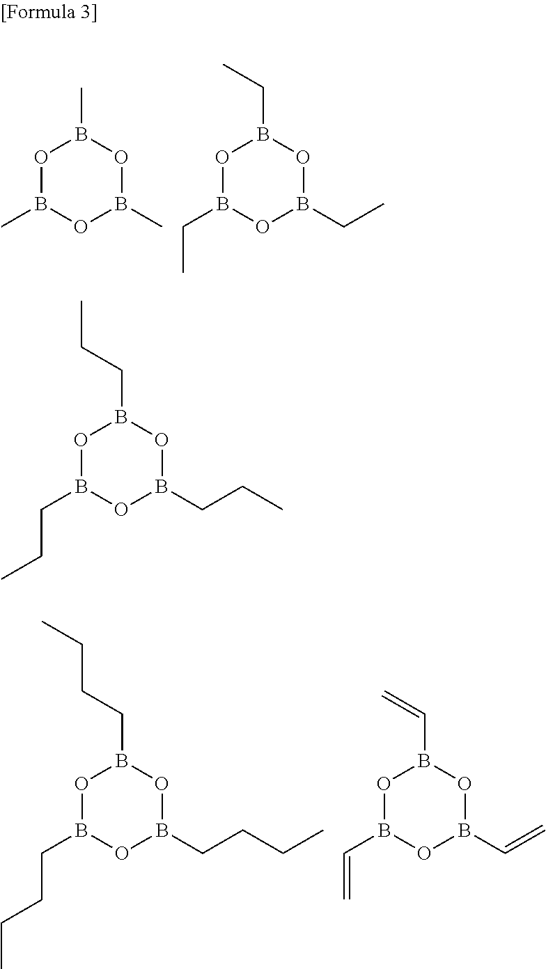
[0147]In examples 1 to 22, the compounds A2, A4, A10, A13 and A14 described above were used as impurity diffusion components ((A) components). A2, A4, A10 and A13 correspond to the first boron compound (A1) ((A1) components), and A14 corresponds to the second boron compound (A2) ((A2) component).

[0148]The types of (A) components described in table 4 below were individually dissolved in butyl acetate so as to have concentrations described in table 4 below, and thus the diffusing agent compositions of examples 1 to 22 were obtained.

[0149]On the surface of the silicon substrate (6 inches, n-type) having the flat surface, the diffusing agent compositions of examples 1 to 22 were individually applied with the spin coater, and thus coating films having film thicknesses described in table 4 were formed. As the silicon substrate, the substrate was used in which the natural oxide film on its surface was removed by immersion in the hydrofluoric acid aqueous solution having a concentration of ...

examples 23 to 29

[0153]In examples 23 to 29, the compounds A2, A4 and A14 described above were used as impurity diffusion components ((A) components). A2 and A4 correspond to the first boron compound (A1) ((A1) components), and A14 corresponds to the second boron compound (A2) ((A2) component).

[0154]The types of (A) components described in table 5 below were individually dissolved in butyl acetate so as to have concentrations described in table 5 below, and thus the diffusing agent compositions of examples 23 to 29 were obtained.

[0155]On the surface of the silicon substrate (6 inches, n-type) having the flat surface, the diffusing agent compositions of examples 23 to 29 were individually applied with the spin coater, and thus coating films having film thicknesses described in table 5 were formed. As the silicon substrate, the substrate was used in which the natural oxide film on its surface was removed by immersion in the hydrofluoric acid aqueous solution having a concentration of 0.5% by mass. Dur...


PUM

PropertyMeasurementUnit
temperatureaaaaaaaaaa
thicknessaaaaaaaaaa

Abstract

A diffusing agent composition and a method of manufacturing a semiconductor substrate using the diffusing agent composition. The diffusing agent composition contains an impurity diffusion component (A) including a first type of boron-containing compound and a second type of boron-containing compound.

Description

[0001]This application claims priority to Japanese Patent Application No. 2017-123646, filed Jun. 23, 2017, and Japanese Patent Application No. 2018-028286, filed Feb. 20, 2018, the entire contents of which are incorporated herein by reference.BACKGROUND OF THE INVENTIONField of the Invention[0002]The present invention relates to a diffusing agent composition which is used for diffusing an impurity diffusion component into a semiconductor substrate and a method of manufacturing a semiconductor substrate using the diffusing agent composition.Related Art[0003]Semiconductor substrates used in semiconductor elements such as transistors, diodes and solar batteries are manufactured by diffusing impurity diffusion components such as phosphorus and boron into the semiconductor substrates. With respect to the semiconductor substrates described above, when a semiconductor substrate for a multi-gate element such as a Fin-FET or a nanowire FET is manufactured, for example, an impurity may be di...

Claims


Application Information

Patent Timeline
Patent Type & Authority Patents(United States)
IPC IPC(8): C08K3/38H01L21/225C09D133/06C08K5/55H01L29/78
CPCH01L21/2254C08K3/38C08K5/55H01L29/785C09D133/06H01L21/2225H01L29/66803C09D4/00C09K3/00H01L21/02052H01L21/22H01L21/324
Inventor SAWADA, YOSHIHIRO
Owner TOKYO OHKA KOGYO CO LTD
Why Eureka
Try Eureka