
Process for forming resist pattern, semiconductor device and manufacturing method for the same

Inactive Publication Date: 2008-02-21
FUJITSU LTD
View PDF29 Cites 41 Cited by
  • Summary
  • Abstract
  • Description
  • Claims
  • Application Information

AI Technical Summary

Benefits of technology

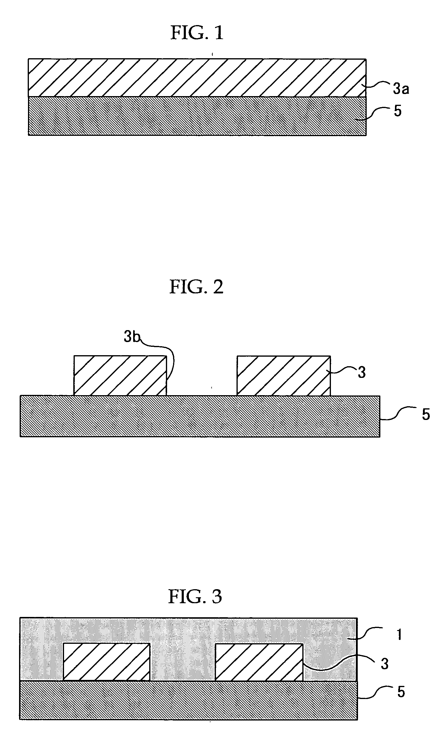
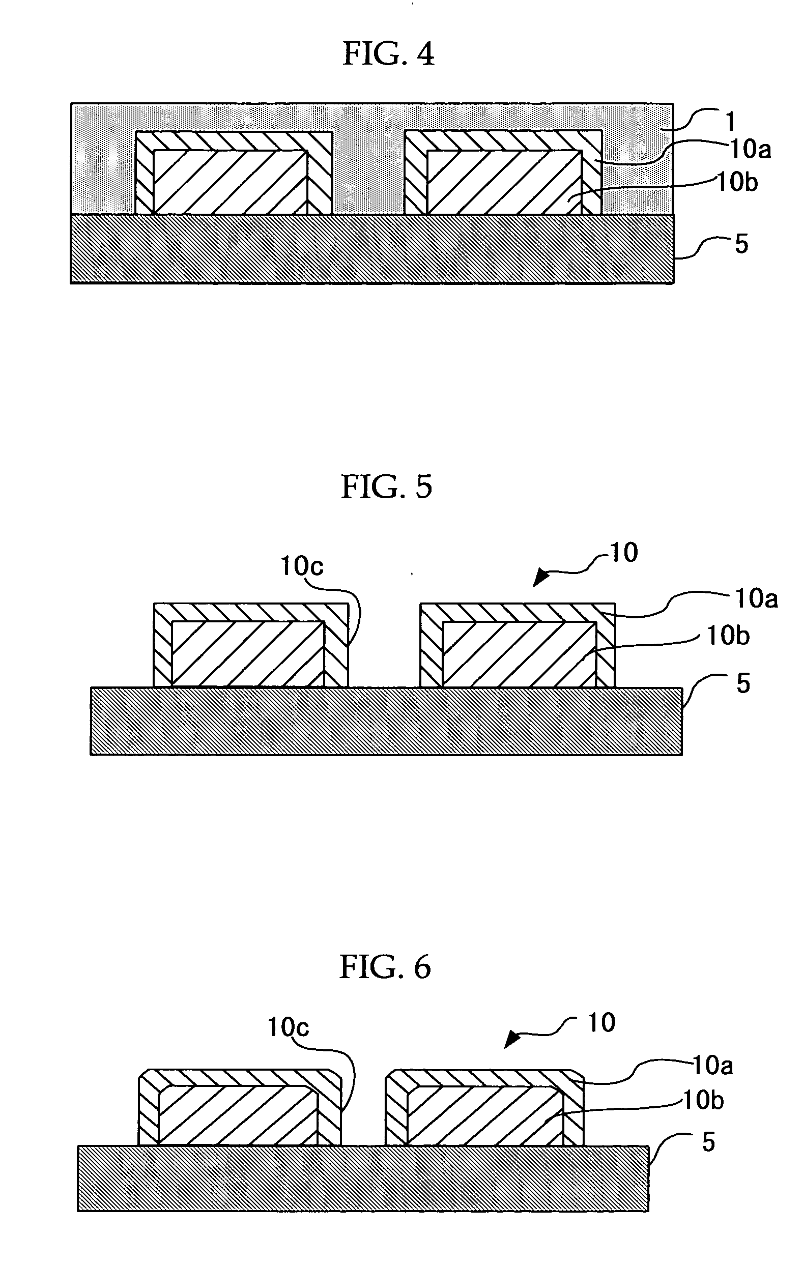
[0022]When the resist pattern thickening material is applied over the resist pattern and heated in the resist pattern thickening step of the resist pattern forming process, the resist pattern thickening material infiltrates the resist pattern at their interface to interact (mix) with the resist pattern material. At this point the resist pattern thickening material has excellent compatibility with the resist pattern and thus results in an efficient formation of a surface layer (mixing layer), a layer in which the resist pattern thickening material and the resist pattern are mixed, on the surface of the resist pattern which now serves as an inner layer. In this way the resist pattern is efficiently thickened by means of the resist pattern thickening material. The resist pattern thus thickened (hereinafter referred to as “swelled” in some cases) is uniformly thickened by means of the resist pattern thickening material (hereinafter such a resist pattern may be referred to as “thickened resist pattern” in some cases). Note that since the resist pattern thickening material contains a compound represented by the general formula (1), it thickens the resist pattern uniformly regardless of the size or constitutional material of the resist pattern. This means that thickening capability of the resist pattern thickening material is less dependent on the size or type of the resist pattern. Furthermore, since the compound represented by the general formula (1) contains an aromatic ring, the resist pattern thickening material is excellent in terms of etching resistance.
[0023]Subsequently, the thickened resist pattern is further heated (baked) in the heating step. At this point, the resin constituting the resist pattern is fluidized, whereby spaces between adjacent pattern lines are narrowed. As a result, it is made possible to easily form a thickened resist pattern with high resolution, which is then used for the formation of a line-space pattern in an interconnection layer of LOGIC LSIs where various sizes of resist patterns are utilized in addition to contact hole patterns, and for the formation of multiple equally-shaped repetitive lines in memory devices such as FLASH memories and DRAMs.
[0025]In the resist pattern forming step of this manufacturing method a resist pattern is formed on a surface of a workpiece, where an interconnection pattern or the like is to be formed. This resist pattern is a thickened resist pattern formed by the process of the present invention for forming a resist pattern, and thus is uniformly thickened regardless of its size. Accordingly, the size of the resulting resist space pattern in the thickened resist pattern is further reduced with high precision.
[0026]In the patterning step, the surface is then patterned by etching using the resist patterned that has been thickened in the resist pattern forming step, whereby the surface is finely patterned with high dimension precision, allowing efficient manufacture of a high-performance, high-quality semiconductor device with a very fine pattern (e.g., an interconnection pattern) formed with high dimension precision and accuracy.
[0027]The semiconductor device of the present invention is characterized in that it is manufactured by the manufacturing method of the present invention for manufacturing a semiconductor device. The semiconductor device is of high quality and high performance and has a very fine pattern (e.g., an interconnection pattern) formed with high dimension precision and accuracy.

Problems solved by technology

Acrylic-based resists suitable for ArF light are different in resin composition from conventional KrF resists and thus are relatively difficult to fluidize at conventional temperatures, or relatively low temperatures.
Meanwhile, in a finer resist pattern with small resist pattern portions, such as a pattern of densely arranged lines of 100 nm width or less, the constituent resist resin that undergoes fluidization is small in volume and thus narrowing of the resist space becomes difficult.

Method used


Image

  • Process for forming resist pattern, semiconductor device and manufacturing method for the same
  • Process for forming resist pattern, semiconductor device and manufacturing method for the same
  • Process for forming resist pattern, semiconductor device and manufacturing method for the same

Examples


example 1

—Preparation of Resist Pattern Thickening Material—

[0205]A resist pattern thickening material containing the following ingredients was prepared:

(1) Polyvinyl alcohol resin (“PVA-205C” by KURARAY Co., Ltd.)

[0206]. . . 4 parts

(2) 2-Hydroxybenzyl alcohol (by Aldrich)

. . . 1 Part

(3) Surfactant (“TN-80” by ADEKA)

. . . 0.06 Parts

(4) Purified water

. . . 96 Parts

—Formation of Resist Pattern—

[0207]An ArF acrylic resist (“AR1244J” by JSR) of 220 nm thickness was applied on an 8-inch silicon substrate (manufactured by Shin-Etsu Chemical Co., Ltd.) on which an antireflective film (“ARC-39” by Nissan Chemical Industries, Ltd.) had been formed by coating. The ArF acrylic resist was exposed to ArF excimer laser using an ArF excimer exposure device to form a hole pattern with an initial pattern size of about 94 nm (pitch=200 nm).

[0208]The resist pattern thickening material prepared above was applied on the hole pattern by spin coating at 1,000 rpm for 5 seconds and then at 3,500 rpm for 40 seconds,...

example 2

[0221]As shown in FIG. 9, an interlayer dielectric film 12 was formed on a silicon substrate 11 and, as shown in FIG. 10, a titanium film 13 was formed on the interlayer dielectric film 12 by sputtering. Next, as shown in FIG. 11, a resist pattern 14 was formed by known photolithography and the titanium film 13 was patterned via reactive ion etching while using the resist pattern 14 as a mask, forming an opening 15a. Subsequently, the resist pattern 14 was removed by reactive ion etching and, as shown in FIG. 12, an opening 15b was formed in the interlayer dielectric film 12 while using the titanium film 13 as a mask.

[0222]The titanium film 13 was removed by wet process and, as shown in FIG. 13, a TiN film 16 was formed on the interlayer insulating film 12 by sputtering, followed by deposition of a Cu film 17 on the TiN film 16 by electroplating. As shown in FIG. 14, chemical and mechanical polishing (CMP) was then performed, leaving barrier metal and a Cu film (first metal film) on...


PUM


Abstract

To provide a process for forming a resist pattern, which the process can adopt even ArF excimer laser light as exposure light in a patterning step, can thicken a resist pattern (e.g., a hole pattern) regardless of its size, and can reduce the size of a resist space pattern with high precision while preventing changes in the resist pattern shape, to thereby make this process easy, inexpensive and efficient while exceeding the exposure (resolution) limits of light sources of exposure devices. The process of the present invention for forming a resist pattern includes: forming a resist pattern; applying over a surface of the resist pattern a resist pattern thickening material; heating the resist pattern thickening material to thicken the resist pattern followed by development; and heating the resist pattern which has been thickened.

Description

CROSS-REFERENCE TO RELATED APPLICATIONS[0001]This application is based upon and claims the benefits of the priority from the prior Japanese Patent Application No. 2006-222310 filed on Aug. 17, 2006, the entire contents of which are incorporated herein by reference.BACKGROUND OF THE INVENTION[0002]1. Field of the Invention[0003]The present invention relates to a process for forming a resist pattern, in which a fine space pattern is formed by thickening a resist pattern upon manufacturing of a semiconductor device while exceeding the exposure (resolution) limits of existing exposure devices. The present invention also relates to a semiconductor and a manufacturing method for the same.[0004]2. Description of the Related Art[0005]Semiconductor integrated circuits have been highly integrated, and thus LSIs and VLSIs are put into practical use. Accompanying this trend, interconnection patterns have also been downsized. A lithographic technique is of great utility in forming fine interconn...

Claims


Application Information

Patent Timeline
IPC IPC(8): G03C5/00
CPCG03F7/40G03F7/11
Inventor NOZAKI, KOJIKOZAWA, MIWA
Owner FUJITSU LTD
Learn More