Pattern for evaluating electric characteristics, method for evaluating electric characteristics, method for manufacturing semiconductor device and method for providing reliability assurance

a technology for electric characteristics and reliability assurance, which is applied in the direction of semiconductor/solid-state device testing/measurement, instruments, measurement devices, etc., can solve the problems of reducing the accuracy of predicting the lifetime of tddb, increasing leakage current, and increasing the probability of dielectric breakdown. , to achieve the effect of shorter time and higher accuracy

Inactive Publication Date: 2008-02-14
RENESAS ELECTRONICS CORP
View PDF5 Cites 20 Cited by
  • Summary
  • Abstract
  • Description
  • Claims
  • Application Information

AI Technical Summary

Benefits of technology

[0016]According to the present invention, the pattern for evaluating electric characteristics that is capable of providing a prediction of the TDDB lifetime with higher accuracy in sho...

Problems solved by technology

This is because larger area of the element to be evaluated provides higher probability of causing a dielectric breakdown.
However, larger area of the element to be evaluated also causes an increased leakage current due to a tunnel effect caused therefrom.
Then, a problem is occur...

Method used


Image

  • Pattern for evaluating electric characteristics, method for evaluating electric characteristics, method for manufacturing semiconductor device and method for providing reliability assurance
  • Pattern for evaluating electric characteristics, method for evaluating electric characteristics, method for manufacturing semiconductor device and method for providing reliability assurance
  • Pattern for evaluating electric characteristics, method for evaluating electric characteristics, method for manufacturing semiconductor device and method for providing reliability assurance

Examples


Embodiment Construction

[0026]The invention will be now described herein with reference to illustrative embodiments. Those skilled in the art will recognize that many alternative embodiments can be accomplished using the teachings of the present invention and that the invention is not limited to the embodiments illustrated for explanatory purposed.

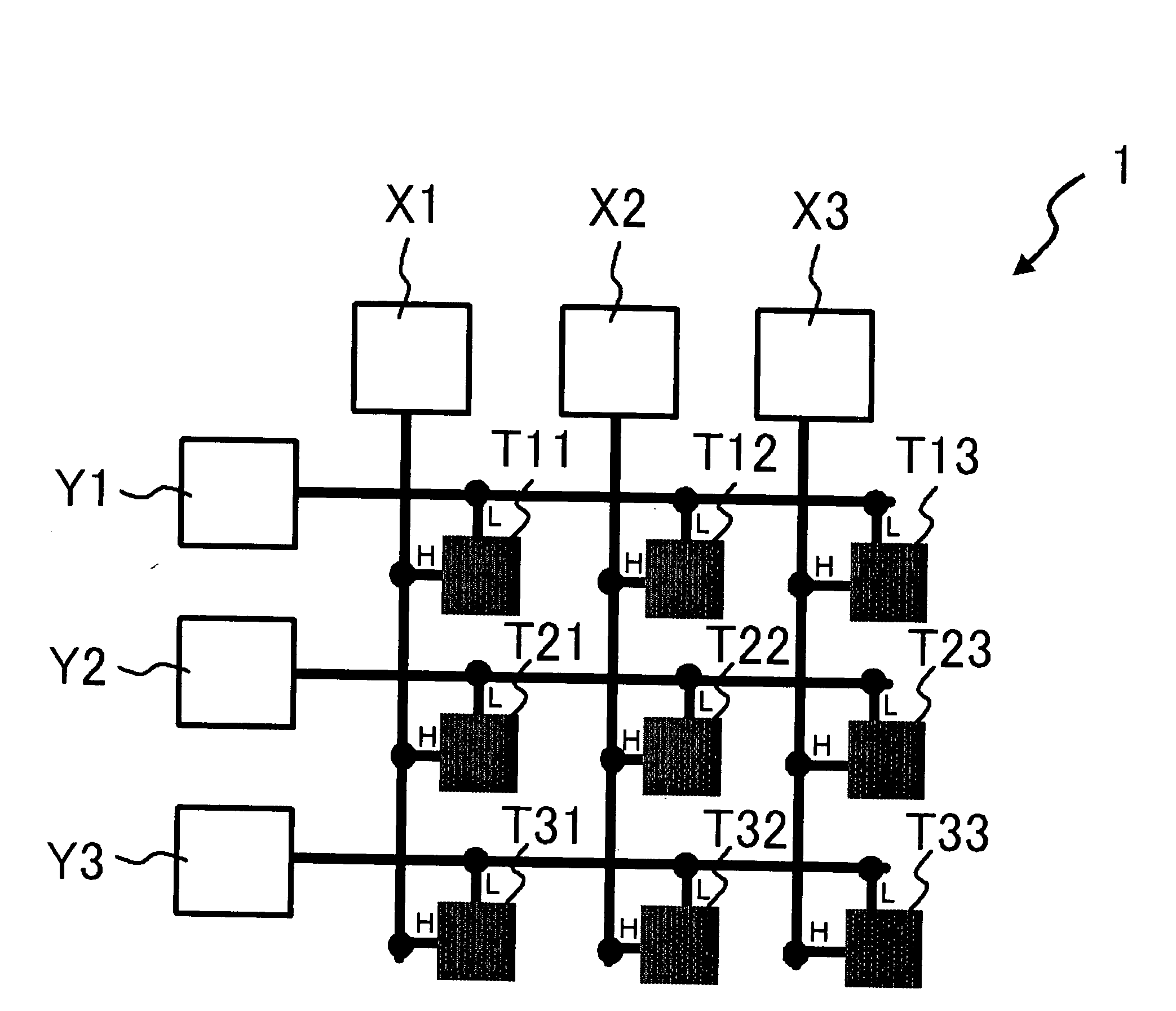
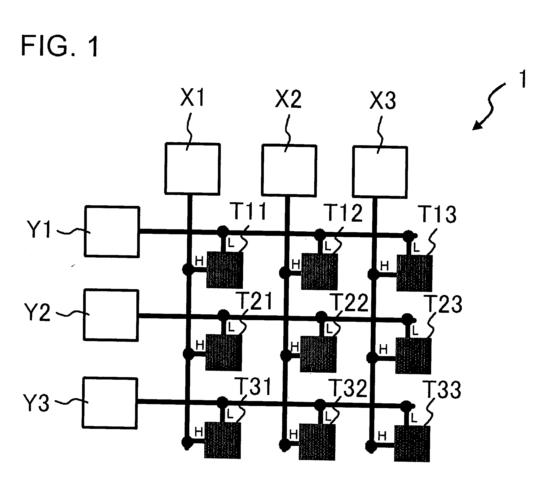
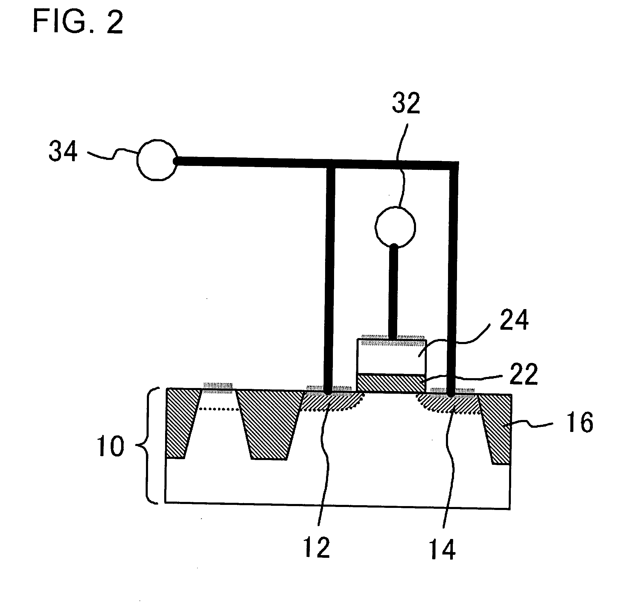
[0027]Preferable exemplary implementations of patterns for evaluating electric characteristics, methods for evaluating electrical characteristics, methods for manufacturing semiconductor devices and methods for providing reliability assurances according to the present invention will be described in reference to the annexed figures. In all figures, identical numeral is assigned to an element commonly appeared in the description of the present invention in reference to the figures, and the detailed description thereof will not be repeated. In the present embodiment, the descriptions will be made in reference to n-type MOS transistors, for the purpose of avoiding de...


PUM


Abstract

An increased area of an element transistor to be evaluated causes an increased leakage current due to a tunnel effect, leading to a reduced accuracy in predicting a TDDB lifetime. A test element group (TEG) 1 is a pattern for evaluating electric characteristics, comprising a plurality of unit transistors T11, T12, T13, T21, T22, T23, T31, T32, T33, which are arranged so as to form a lattice-shaped pattern. Each of the unit transistors comprises a gate dielectric serving as an object to be evaluated, and source region and drain region, which are a short-circuited.

Description

[0001]This application is based on Japanese patent application No. 2006-219,287, the content of which is incorporated hereinto by reference.BACKGROUND[0002]1. Technical Field[0003]The present invention relates to a pattern for evaluating electric characteristics, a method for evaluating electric characteristics, a method for manufacturing a semiconductor device and a method for providing a reliability assurance.[0004]2. Related Art[0005]The characteristic of TDDB lifetime (time dependent dielectric breakdown) of a gate dielectric is one of factors for representing reliability of semiconductor devices, and is required to be assured at a real operating voltage. Therefore, it is critical to precisely predict such TDDB lifetime, in view of providing semiconductor devices that exhibit an improved reliability. Typical technologies for providing predictions of the TDDB lifetime by employing a pattern for evaluating electric characteristics are disclosed in Japanese Patent Laid-Open No. 200...

Claims


Application Information

Patent Timeline
IPC IPC(8): H01L21/66G01R31/26
CPCG01R31/2884G01R31/2623
Inventor KOYAMA, SHINTOGO, MITSUHIRO
Owner RENESAS ELECTRONICS CORP
Why Eureka
Try Eureka