
Electrode Pattern For Resistance Heating Element and Wafer processing Apparatus

a technology of heating element and electrode pattern, which is applied in the direction of transportation and packaging, paper/cardboard containers, workpiece holders, etc., to achieve uniform heating temperature distribution

Active Publication Date: 2008-02-07
GENERAL ELECTRIC CO
View PDF6 Cites 61 Cited by
  • Summary
  • Abstract
  • Description
  • Claims
  • Application Information

AI Technical Summary

Benefits of technology

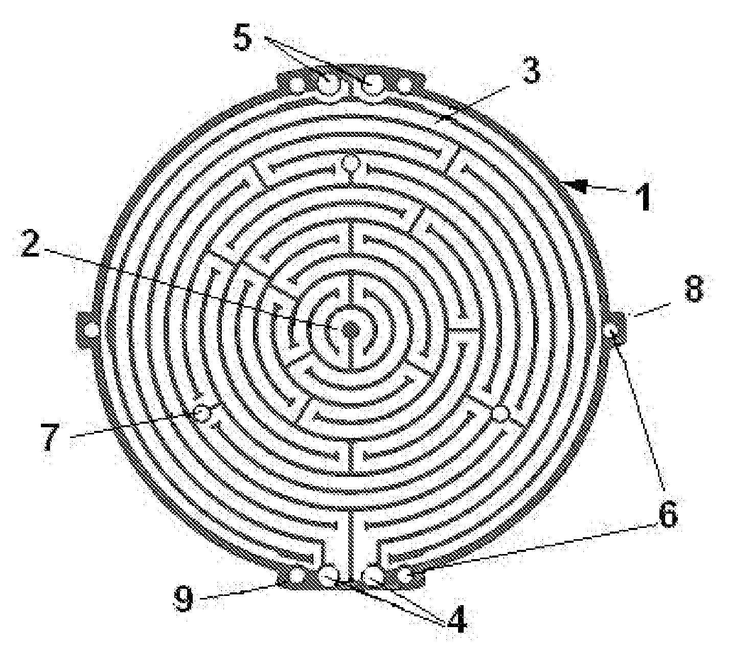
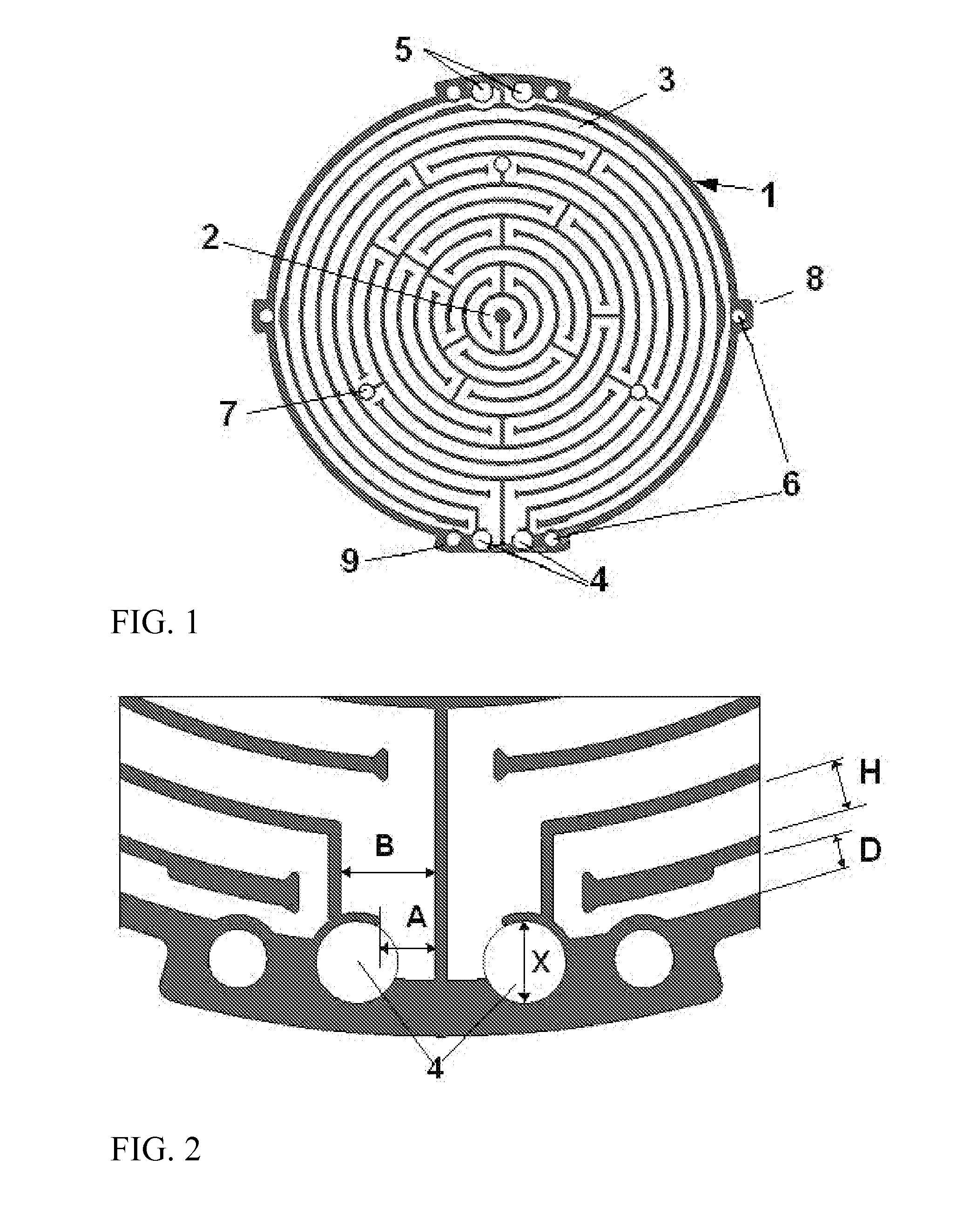
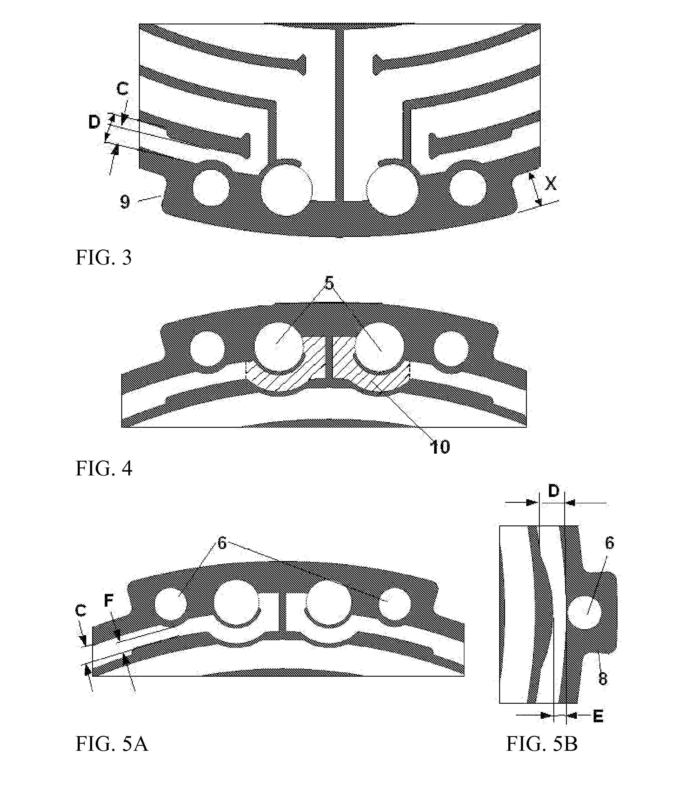
[0008]In another aspect of the invention, the electrode pattern is optimized for a wafer processing apparatus having relative large tabs. Due to structure limitation of a tab, electrodes typically do not extend to cover the surface of the tabs. In one embodiment, the width of the outermost electrode path is reduced to a range from 0.5 to 0.95 of its original width, for an adjusted width reduction such that the main heater area is insulated from the heat loss at the tabs allowing uniform surface temperature to heat the wafer.
[0010]In yet another aspect, the invention relates to a wafer processing apparatus having a multi-zone heater pattern with different geometries and specification for each zone, operating in a non-uniform boundary condition environment but still obtaining uniform heater temperature distribution. In the heater, the two heating zones are designed to compensate for the additional heat loss on the outer peripheral edge of the heater provide radial temperature uniformity, with the outermost path in the first zone has a width ranging from 0.6 to 0.95 of the width of the inner path in the second zone of the electrode.

Problems solved by technology

Due to structure limitation of a tab, electrodes typically do not extend to cover the surface of the tabs.

Method used


Image

  • Electrode Pattern For Resistance Heating Element and Wafer processing Apparatus
  • Electrode Pattern For Resistance Heating Element and Wafer processing Apparatus
  • Electrode Pattern For Resistance Heating Element and Wafer processing Apparatus

Examples


second embodiment

[0033]In a second embodiment, the protective coating layer 25 comprises a high thermal stability zirconium phosphates, having the NZP structure. The term NZP refers to NaZr2 (PO4)3, as well as to related isostructural phosphates and silicophosphates having a similar crystal structure. These materials in one embodiment are prepared by heating a mixture of alkali metal phosphates or carbonates, ammonium dihydrogen phosphate (or diammonium phosphate) and tetravalent metal oxides.

[0034]In one embodiment, the NZP-type coating layer 25 has a general formula: (L,M1,M2,Zn,Ag,Ga,In,Ln,Y,Sc)1, (Zr,V,Ta,Nb,Hf,Ti,Al,Cr,Ln)m (P,Si,VAl)n(O,C,N)12 wherein L=alkali, M1=alkaline earth, M2=transition metal, Ln=rare earth and the values of l, m, n are so chosen that a charge balance is maintained. In one embodiment, the NZP-type protective coating layer 25 includes at least one stabilizer selected from the group of alkaline earth oxides, rare earth oxides, and mixtures thereof. Examples include yttria...

third embodiment

[0036]In one example, the protective coating layer 25 contains a mixture of SiO2 and a plasma-resistant material comprising an oxide of Y, Sc, La, Ce, Gd, Eu, Dy, or the like, or a fluoride of one of these metals, or yttrium-aluminum-garnet (YAG). Combinations of the oxides of such metals, and / or combinations of the metal oxides with aluminum oxide, may be used. In a third embodiment, the protective coating layer 25 comprises from 1 to 30 atomic % of the element of the group 2a, group 3a or group 4a and from 20 to 99 atomic % of the Si element in terms of an atomic ratio of metal atoms exclusive of oxygen. In one example, the layer 25 includes aluminosilicate glasses comprising from 20 to 98 atomic % of the Si element, from 1 to 30 atomic % of the Y, La or Ce element, and from 1 to 50 atomic % of the Al element, and zirconia silicate glasses comprising from 20 to 98 atomic % of the Si element, from 1 to 30 atomic % of the Y, La or Ce element, and from 1 to 50 atomic % of the Zr elem...


PUM

PropertyMeasurementUnit
Temperatureaaaaaaaaaa

Abstract

There is disclosed a wafer processing apparatus having optimized electrode patterns for its resistive heating element. The optimized electrode pattern is designed to compensate for the heat loss around contact areas, electrical connections, and through-holes, etc., by generating more heat near or around those areas, providing maximum temperature uniformity. In another embodiment of the optimized design of the invention, the resistance of heating element closely matches the impedance of the power supply for higher efficiency, especially when higher operating temperature or higher electrical power is required.

Description

CROSS REFERENCE TO RELATED APPLICATION[0001]This application claims the benefits of U.S. 60 / 806,620 filed Jul. 5, 2006, which patent application is fully incorporated herein by reference.FIELD OF INVENTION[0002]The invention relates to a circuit pattern of resistance heating elements embedded in a wafer processing apparatus for use in the manufacture of semiconductors.BACKGROUND OF THE INVENTION[0003]Wafer processing apparatuses are used to treat wafers in film making systems such as plasma CVD, low pressure CVD, optical CVD or PVD systems, or in etching systems based on plasma etching or optical etching technique, particularly, for production of semiconductor devices. Ceramic heaters containing heating elements have been used to support the wafers and substrates and to heat them to a specified treating temperature. The electrode pattern design of heating elements directly affects the performance of the heating unit, which is defined as ramp rate, operating temperature, and most imp...

Claims


Application Information

Patent Timeline
IPC IPC(8): B31B1/60
CPCH05B3/143Y10S269/903H01L21/02
Inventor LU, ZHONG-HAO
Owner GENERAL ELECTRIC CO
Learn More