
Pre-Charge Systems and Methods for ADC Input Sampling

Active Publication Date: 2008-01-31
TEXAS INSTR INC
View PDF1 Cites 15 Cited by
  • Summary
  • Abstract
  • Description
  • Claims
  • Application Information

AI Technical Summary

Benefits of technology

[0014]The invention has one or more advantages potentially including but not limited to providing input driver methods and systems with reduced power requirements, improved SNR, improved SFDR performance, and adaptability for use with various types of ADC systems.

Problems solved by technology

The ADC cannot convert a moving target, necessitating that the sample of the input signal be held for a period of time.
Departures from the ideal occur in practice due to several problems.
In systems having a capacitive load, op amp sampling circuits have inherent instability problems.
Compensation capacitance may be added to offset the phase delay of the capacitive load and keep the system under control, but increasing the compensation capacitor in order to enhance stability has the undesirable side-effect of increasing rise time and reducing bandwidth.
As the resolution and speed of ADCs increases, it becomes increasingly difficult to use an op amp to drive the switching input load of high-speed over-sampling ADCs.
In order to arrive at a satisfactory configuration using an opamp to drive a high performance ADC, it is often necessary for the user to make adjustments to the R and C at the input according to performance measurements, making such solutions costly and application-specific.
The SFDR of the sampled signal in these cases is limited by how fast the input amplifier can settle in response to the step at the output caused by the switching load.
Since the available time to settle is only one half of a clock cycle, it becomes extremely difficult for the amplifier to settle, to 16-18-bit linearity for example, as the clock frequencies increase, and also as the value of capacitor being switched increases.
This approach becomes less effective as the signal frequency increases, since the −3 db bandwidth of the filter has to be increased to prevent signal attenuation, implying that high frequency thermal noise will necessarily also increase.
Moreover, this approach falls short of achieving very good SFDR numbers because the output at the RC filter is a slow moving node and requires a relatively long settling time.
These problems are often encountered in high speed pipelined ADC systems as well as successive approximation register (SAR) ADCs.
Another important practical problem encountered in the arts is that high-speed amplifiers are generally manufactured using BICMOS processes.
If the ADC system is implemented using a slow CMOS process to achieve higher swings, then it may not be practical to integrate very fast amplifiers into the system because of the effect of parasitic capacitances on bandwidth and slew rate.
However, those familiar with the applicable arts will recognize that this approach to the problem presents additional problems from a manufacturing point of view.
One particular disadvantage of this approach is the requirement to use an additional buffer, which means additional power is required.
Another problem is that the power consumption for the pre-charge buffer may be excessive.

Method used


Image

  • Pre-Charge Systems and Methods for ADC Input Sampling
  • Pre-Charge Systems and Methods for ADC Input Sampling

Examples


Embodiment Construction

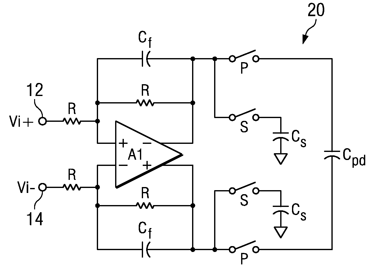
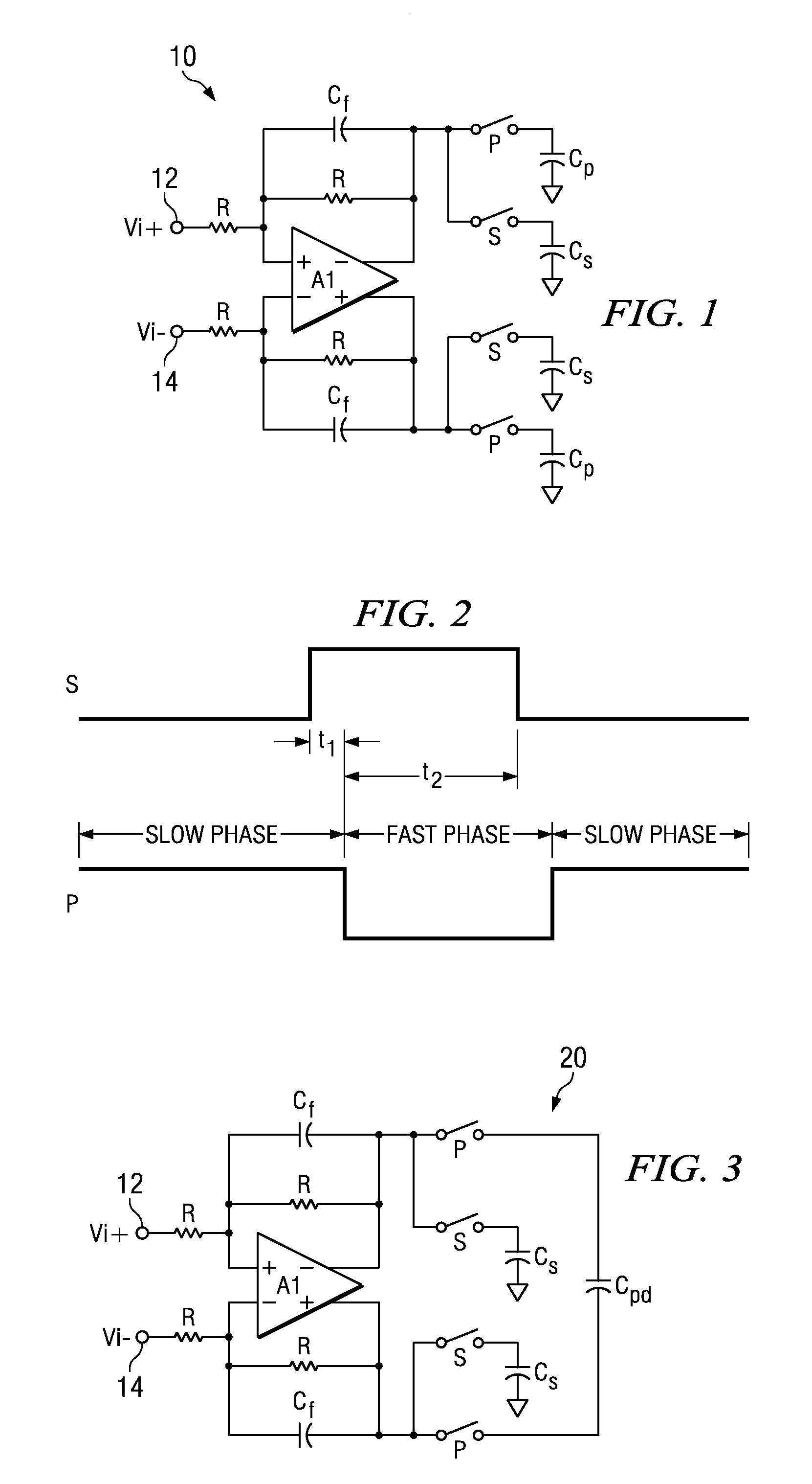
[0020]In general, the invention provides novel pre-charge methods and systems embodied in high performance analog to digital converter input drivers. An exemplary embodiment of the invention is portrayed in the schematic diagram of FIG. 1. An ADC driver system 10 is shown with an op amp A1 for sampling the inputs, 12, 14. For using the system 10 with a high performance ADC, an amplifier A1 that is sufficiently fast and accurate for the application is selected. It may enhance appreciation of the principles of the invention to consider the underlying, but perhaps easily overlooked fact that speed and accuracy are only required of the op amp A1 during the intervals when the ADC system is actually sampling the input. It follows that during the other phase of the operative clock cycle, the amplifier A1 may be used as described. Examining FIG. 1, it may be seen that the system 10 is configured so that during the non-sampling phase of the clock cycle, the amplifier A1 may be operated as a ...


PUM


Abstract

The invention provides methods and systems useful for quickly and accurately sampling a switched capacitive load. Systems are disclosed in which the methods are implemented using an operational amplifier operably coupled to a pre-charge capacitor for storing an input charge. A sampling capacitor is also coupled to the operational amplifier and to the pre-charge capacitor for receiving and holding the input charge. The system is so configured for a coarse sampling phase and a fine sampling phase the to ensure that the sampling capacitor settles quickly to provides an output.

Description

TECHNICAL FIELD[0001]The invention relates to electronic semiconductor devices and manufacturing. More particularly, the invention relates to input drivers for analog to digital converters (ADC) and to systems and methods for implementing the same.BACKGROUND OF THE INVENTION[0002]An analog to digital converter (ADC) system typically uses an input driver circuit to sample an analog signal for input to the converter. Depending on the application, there may be a need to manipulate the signal in various ways in order to make use of the capabilities of the ADC. Op amp circuitry is typically used to perform one or more operations such as inverting, attenuating, multiplying, and shifting the input signal to be operated on by the ADC. The ADC cannot convert a moving target, necessitating that the sample of the input signal be held for a period of time. Ideally, a holding capacitor is instantaneously charged to the input voltage, the sampled charge is held for the ADC, and the sample is then...

Claims


Application Information

Patent Timeline
IPC IPC(8): H03M1/12
CPCG11C27/026
Inventor GUPTA, AMIT KUMARSOUNDARAPANDIAN, KARTHIKEYAN
Owner TEXAS INSTR INC
Learn More