
Schottky gate metallization for semiconductor devices

a technology of semiconductor devices and gate metallization, which is applied in the direction of semiconductor devices, electrical equipment, transistors, etc., can solve the problems of reducing the effective gate-to-channel layer distance, posing a potential threat to the reliable performance of the device, and e-hemts exhibiting high performance and thermal stability

Inactive Publication Date: 2008-01-31
THE BOARD OF TRUSTEES OF THE UNIV OF ILLINOIS
View PDF1 Cites 18 Cited by
  • Summary
  • Abstract
  • Description
  • Claims
  • Application Information

AI Technical Summary

Benefits of technology

[0015] A form of the invention is directed to a method of forming a Schottky barrier contact to a semiconductor material, including the following steps: depositing an iridium contact on a surface of the semiconductor material; and annealing the iridium contact to form a Schottky barrier contact to said semiconductor material. In one preferred embodiment of this form of the invention, the semiconductor material is a III-V semiconductor material, which, in an illustrated embodiment, is InAlAs. The annealing temperature is preferably in the range about 350° C. to 50

Problems solved by technology

While high performance has been more readily achieved in D-HEMTs, it is challenging to fabricate E-HEMTs exhibiting high performance and thermal stability.
In-diffusion of Pt in InAlAs during thermal treatment reduces the effective gate-to-channel layer distance.
Nonetheless, the rapid diffusion of Pt in InAlAs poses a potential threat to the reliable performance of the devices (see S. Kim et al., 2005, supra; M. Dammann et al.
The a-layer consumed up to 70% of the InAlAs barrier layer during prolonged thermal treatment at a low temperature of 250° C. The substantial shortening in the gate-to-channel distance brings considerable changes to the operational parameters of the devices such as transconductance and gate capacitance, or can even cause device failure (see S. Kim et al., 2005, supra; and M. Dammann et al., 2004, supra).
Since it is preferable to have a metallization that is stable after the device is fabricated, the low optimum annealing temperature, fast diffusivity, and thus low thermal stability of Pt, are serious drawbacks to its use for Schottky contacts.

Method used


Image

  • Schottky gate metallization for semiconductor devices
  • Schottky gate metallization for semiconductor devices
  • Schottky gate metallization for semiconductor devices

Examples


Embodiment Construction

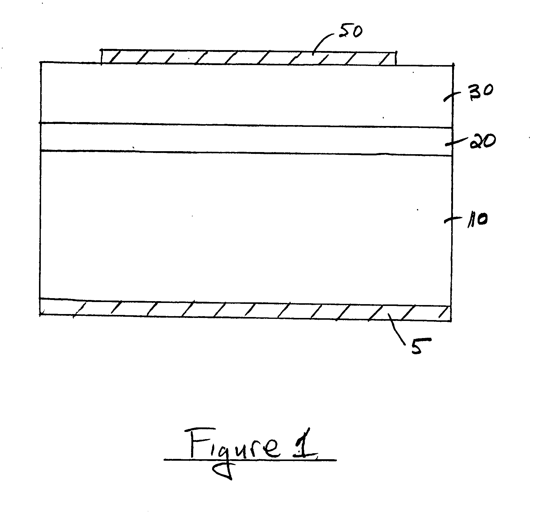
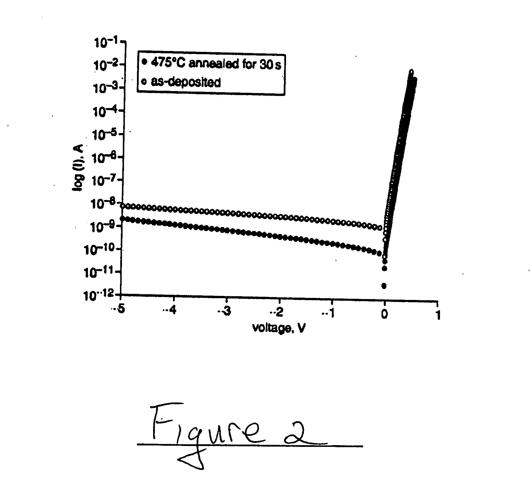
[0027] The layer structure used to fabricate Schottky diodes (see FIG. 1) for an example hereof was grown by molecular beam epitaxy (MBE) on an n+ InP substrate 10. From the bottom up, the structure included a 0.1 μm thick n+ (1×1018 cm−3) InAlAs buffer layer 20 followed by a 0.9 μm-thick, lightly doped InAlAs (n=1×1016 cm−3) layer 30. AuGe / Ni / Au ohmic contact 5 was formed on the backside of the InP by e-beam evaporation and alloying at 370° C. for 60 s in a furnace. 250 μm diameter, circular-shaped Schottky contacts (represented at 50) were fabricated by photolithography, e-beam evaporation and lift-off. Samples were rinsed in HCl:DI=1:2 solution to remove native oxide before metallization. Samples with 15 nm-thick Ir and Pt contacts were fabricated. Some of these samples were thermally treated at various temperatures ranging from 150 to 500° C. for 30 s in nitrogen ambient in a rapid thermal anneal system. DC I-V-T measurements were performed on the samples on a variable temperatu...


PUM


Abstract

A method of forming a Schottky barrier contact to a semiconductor material, includes the following steps: depositing an iridium contact on a surface of the semiconductor material; and annealing the iridium contact to form a Schottky barrier contact to the semiconductor material. For an example of an iridium Schottky contact on an InAlAs semiconductor material, the annealing temperature is preferably in the range about 350° C. to 500° C.

Description

RELATED APPLICATIONS [0001] Priority is claimed from U.S. Provisional Patent Application No. 60 / 808,440, filed May 24, 2006, and U.S. Provisional Patent Application No. 60 / 808,478, filed May 24, 2006, and both said U.S. Provisional Patent Applications are incorporated herein by reference. The subject matter of the present Application is related to subject matter disclosed in copending U.S. patent application Ser. No. ________ (File UI-TF-06074), filed of even date herewith, and assigned to the same assignee as the present Application. GOVERNMENT RIGHTS [0002] This invention was made with Government support under Contract Number ANI-0121662 awarded by the National Science Foundation (NSF) and Contract Number N00014-01-1-0018 awarded by Office of Naval Research (ONR). The Government has certain rights in the invention.FIELD OF THE INVENTION [0003] This invention relates to the field of semiconductor devices and methods and, more particularly, to Schottky barrier contacts for semicondu...

Claims


Application Information

Patent Timeline
IPC IPC(8): H01L29/739H01L21/28H01L29/80H01L21/338
CPCH01L21/8252H01L27/0605H01L27/0883H01L29/872H01L29/475H01L29/7784H01L27/095
Inventor ADESIDA, ILESANMIKIM, SEIYONWANG, LIANG
Owner THE BOARD OF TRUSTEES OF THE UNIV OF ILLINOIS
Learn More