Multi-functional chalcogenide electronic devices having gain
- Summary
- Abstract
- Description
- Claims
- Application Information
AI Technical Summary
Benefits of technology
Problems solved by technology
Method used
Image
Examples
example 1
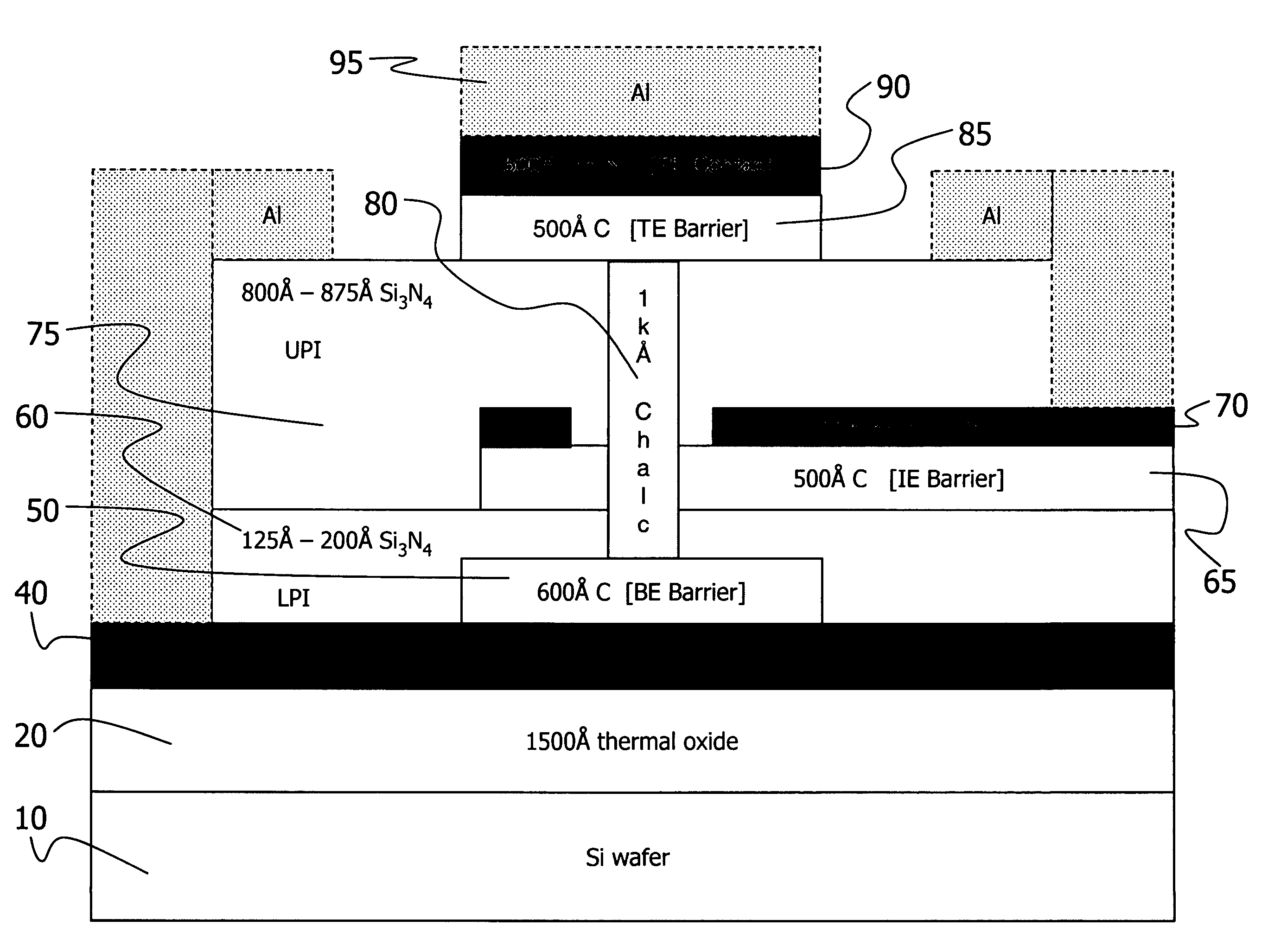
[0064]An example of a device structure according to the instant invention is shown in FIG. 3. FIG. 3 shows a cross-sectional view of a three terminal device structure. A plurality of these devices was formed on a silicon wafer. The devices and layers on the wafer were formed using conventional sputter deposition, etching, and lithography techniques. The structure includes a silicon wafer substrate 10, a silicon oxide layer 20, a bottom terminal that includes a conductive layer 40 formed from Mo and a carbon layer 50, a lower Si3N4 insulating region 60, a control terminal that includes a carbon layer 65 and a Mo layer 70, an upper Si3N4 insulating layer 75, a chalcogenide material 80 contained in the pore region of the device, a top terminal that includes a carbon layer 85 and a conductive layer 90 that includes Mo, and Al layers 95. In this example, the chalcogenide material 80 is an Se—Te chalcogenide alloy having an approximate composition Si5Ge11As28Te34Se21S. Typical layer thick...
example 2
[0066]In this example, a device having a symmetric design was fabricated according to the process described in EXAMPLE 1 hereinabove. In the symmetric design, the upper insulating layer 75 and lower insulating layer 60 both had a thickness of 500 Å, so that the control terminal 70 was positioned symmetrically between top terminal 90 and lower terminal 30. Other features of the symmetric device are as described in EXAMPLE 1. The separation between control terminal 70, top terminal 90 and lower terminal 30 is believed to be large enough to prevent a significant interaction between the space-charge regions emanating from the three terminals.
example 3
[0067]In this example, a demonstration of the latching and non-latching modes of operation of the device described in EXAMPLE 1 is provided. An illustration of operation in latching mode is presented in FIG. 4, which shows the time variation of the voltage between the top and bottom terminals of the device before and after application of a voltage signal between the control terminal and bottom terminal. FIG. 4 includes two data curves: one, depicted in diamond symbols, that shows the voltage between the top and bottom terminals as a function of time and another, depicted in square symbols, that shows the voltage between the control and bottom terminals as a function of time. At the outset of the experiment, a signal of approximately 2V was applied between the top and bottom terminals and no signal was applied between the control terminal and the bottom terminal. The signal applied between the top and bottom terminals was an insufficient voltage to cause a switching event to occur. W...
PUM
 Abstract
Description
Claims
Application Information
 - R&D
- Intellectual Property
- Life Sciences
- Materials
- Tech Scout
- Unparalleled Data Quality
- Higher Quality Content
- 60% Fewer Hallucinations
Browse by: Latest US Patents, China's latest patents, Technical Efficacy Thesaurus, Application Domain, Technology Topic, Popular Technical Reports.
© 2025 PatSnap. All rights reserved.Legal|Privacy policy|Modern Slavery Act Transparency Statement|Sitemap|About US| Contact US: help@patsnap.com


