
Three terminal magnetic sensing devices having base lead layers in-plane with collector substrate materials and methods of making the same

a technology of base lead layer and collector substrate material, which is applied in the field of three-terminal magnetic sensors, can solve the problems of unnecessarily large track width, fragile and susceptible to damage of sensor stack structure, etc., and achieve the effect of increasing the number of areal recording

Inactive Publication Date: 2007-10-11
WESTERN DIGITAL TECH INC
View PDF20 Cites 4 Cited by
  • Summary
  • Abstract
  • Description
  • Claims
  • Application Information

AI Technical Summary

Benefits of technology

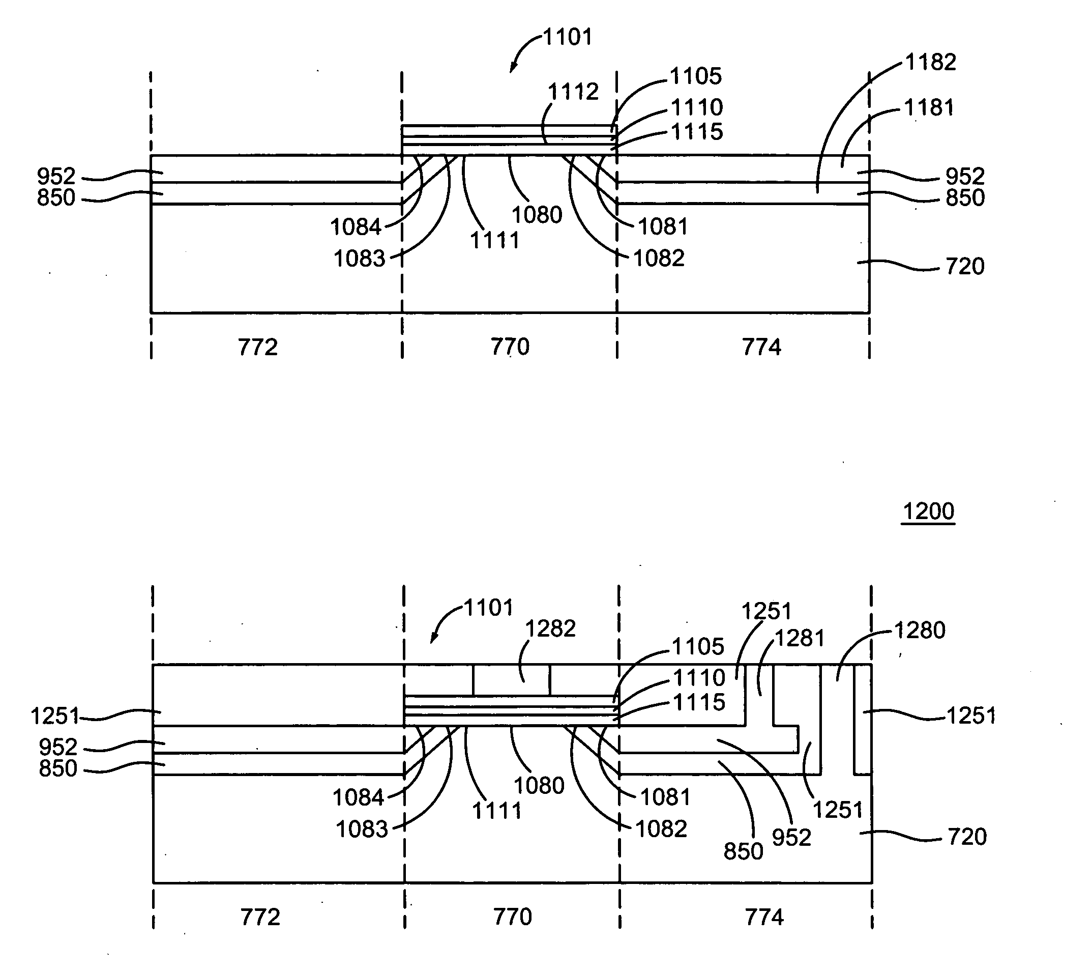
[0013] Advantageously, the base conductive via formation may occur without causing damage to the sensor stack structure. Also, the base lead layer is formed in the recessed region of the collector substrate prior to the formation of the sensor stack structure such that the TTM may be entirely in-situ manufactured. Furthermore, the trackwidth of the TTM is defined directly by the elevated region of the collector substrate. The TTM is suitable for incorporation into nanoscale devices which increase areal recording densities, therefore aiding the revolution in magnetic storage.

Problems solved by technology

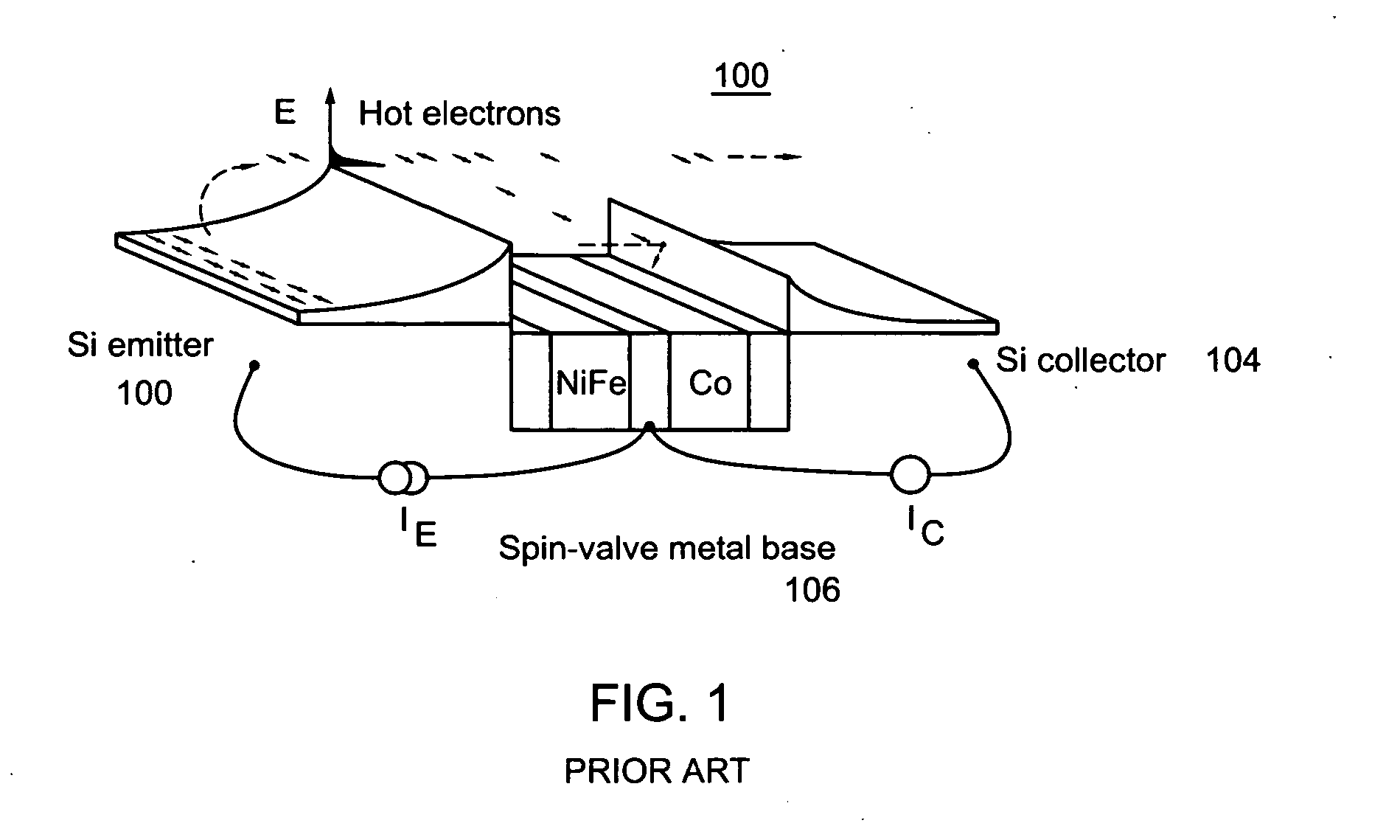
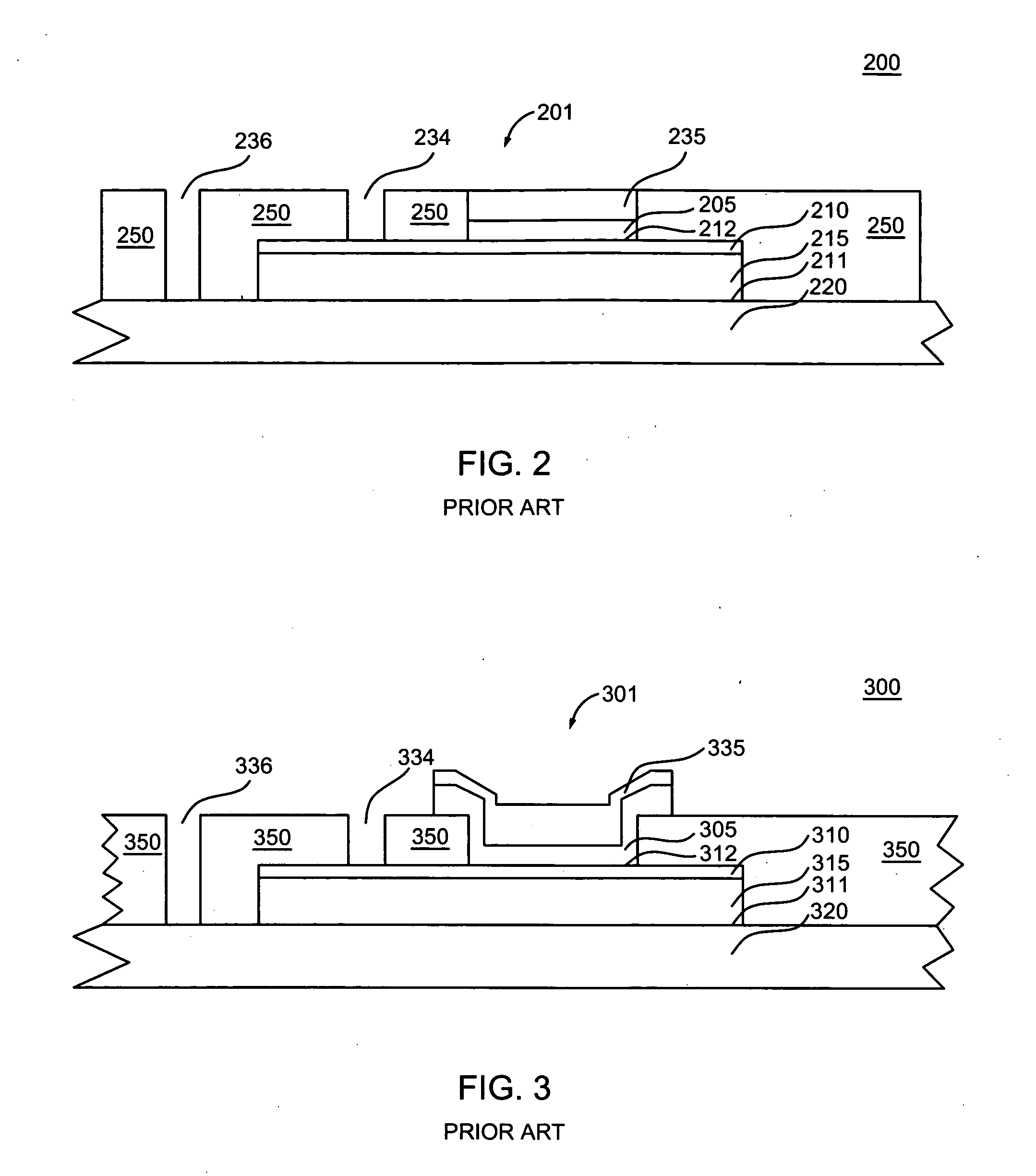
In general, sensor stack structures are fragile and susceptible to damage due to ion bombardment and chemical exposure during manufacturing steps such as those used in the formation of conductive vias for connecting TTM base regions to their terminals.
As a result, the trackwidths are unnecessarily large due to the relatively long length of the base regions.

Method used


Image

  • Three terminal magnetic sensing devices having base lead layers in-plane with collector substrate materials and methods of making the same
  • Three terminal magnetic sensing devices having base lead layers in-plane with collector substrate materials and methods of making the same
  • Three terminal magnetic sensing devices having base lead layers in-plane with collector substrate materials and methods of making the same

Examples


Embodiment Construction

[0028] Three terminal magnetic sensing devices (TTMs) having base lead layers in-plane with collector substrate materials, and methods of making the same, are disclosed. In one illustrative example, a collector substrate having an elevated region and a recessed region adjacent the elevated region is provided. An insulator layer is formed in full-film over the collector substrate, and a base lead layer is formed in full-film over the insulator layer and in-plane with semiconductor materials of the elevated region. The insulator materials and the base lead materials formed over the elevated region are then removed. Next, a sensor stack structure having an emitter region and a base region is formed over the elevated region such that part of the base region is formed over an end of the base lead layer. A base conductive via may be formed to contact base lead materials of the base lead layer at a suitable distance away from the sensor stack structure. Advantageously, the base conductive ...


PUM


Abstract

Three terminal magnetic sensing devices (TTMs) having base lead layers in-plane with collector substrate materials, and methods of making the same, are disclosed. In one illustrative example, a collector substrate having an elevated region and a recessed region adjacent the elevated region is provided. An insulator layer is formed in full-film over the collector substrate, and a base lead layer is formed in full-film over the insulator layer and in-plane with semiconductor materials of the elevated region. The insulator materials and the base lead materials that are formed over the elevated region are removed. A sensor stack structure having an emitter region and a base region is then formed over the elevated region such that part of the base region is formed over an end of the base lead layer. A base conductive via may be formed to contact base lead materials of the base lead layer at a suitable distance away from the sensor stack structure. Advantageously, the base conductive via formation may occur without causing damage to the sensor stack structure. Also, the base lead layer is formed in the recessed region of the collector substrate prior to the formation of the sensor stack structure such that the TTM may be entirely in-situ manufactured. Furthermore, the trackwidth of the TTM may be defined directly by the elevated region of the collector substrate. The TTM is suitable for incorporation into nanoscale devices which increase areal recording densities, therefore aiding the revolution in magnetic storage.

Description

BACKGROUND [0001] 1. Field of the Technology [0002] The present application relates generally to three terminal magnetic sensors (TTMs) suitable for use in magnetic heads, and more specifically to TTMs having base lead layers in-plane with collector substrate materials. [0003] 2. Description of the Related Art [0004] Magnetoresistive (MR) sensors have typically been used as read sensors in hard disk drives. An MR sensor detects magnetic field signals through the resistance changes of a read element, fabricated of a magnetic material, as a function of the strength and direction of magnetic flux being sensed by the read element. The conventional MR sensor, such as that used as a MR read head for reading data in magnetic recording disk drives, operates on the basis of the anisotropic magnetoresistive (AMR) effect of the bulk magnetic material, which is typically permalloy. A component of the read element resistance varies as the square of the cosine of the angle between the magnetizati...

Claims


Application Information

Patent Timeline
Patent Type & Authority Applications(United States)
IPC IPC(8): H01L21/00
CPCB82Y10/00B82Y25/00H01L29/66984G11B5/3903G11B5/398G01R33/093
Inventor FONTANA, ROBERT E. JR.LI, JUI-LUNGLILLE, JEFFREY S.NICOLETTI, SERGIO
Owner WESTERN DIGITAL TECH INC
Learn More