Bonding Wire and Integrated Circuit Device Using the Same
a technology of integrated circuit devices and bonding wires, which is applied in the direction of manufacturing tools, non-electric welding apparatuses, and capacitors, etc., can solve the problems of reducing bond reliability, unstable reproducibility of ball shape, and degrading bonding quality, and achieves excellent ball shape stability, excellent drawability, and advantageous production cost and bonding characteristics.
- Summary
- Abstract
- Description
- Claims
- Application Information
AI Technical Summary
Benefits of technology
Problems solved by technology
Method used
Image
Examples
example 1
[0091] A coating was formed to a thickness of 0.8 μm by electroplating on a core copper wire having a purity of 99.995% and a diameter of 200 μm. By drawing and annealing this wire, various kinds of bonding wires were produced, each having a core diameter of 25.2 μm and a coating layer thickness of 0.1 μm. Using each wire, 100 balls of diameter 60 μm were formed by using a bonder (Model FB137 manufactured by Kaijo corporation), and the number of occurrences of a shape defect in which the center of the ball was displaced from the center of the wire was examined. The results are shown in Table 1 along with the core materials and coating materials used.
[0092] Wet contact angle at the time of core material melting was measured in the following manner by using high temperature wettability test equipment WET1200 manufactured by ULVAC-RIKO.
[0093] A lump of material produced by compressing a 2.5-mm size ball of core material into an easily mountable shape was placed on a sheet of coating ...
example 2
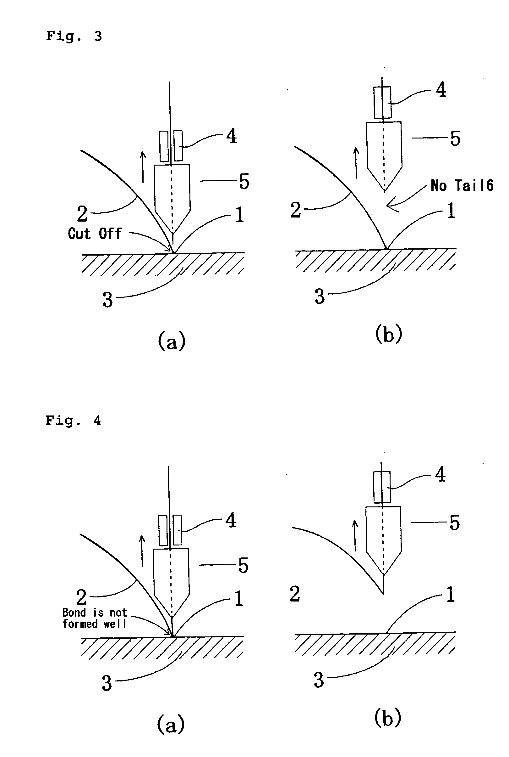
[0095] (1) A film of gold strike plating was formed to a thickness of about 0.04 μm by strike electroplating on a copper wire having a purity of 99.995% and a diameter of 200 μm. After which a film of palladium plating was formed to a thickness of 0.8 μm. By drawing and annealing this wire, copper bonding wires were produced, each having a copper core diameter of 25.2 μm, a palladium layer (coating layer) thickness of 0.1 μm, a gold layer (different metal layer) thickness of about 0.005 μm, and an elongation of 15%. By adjusting the diameter of the guide roller and the tensile force used to wind the wire around a spool, samples with various curvature radiuses were produced. Using each sample, bonding was performed on a 208-pin QFP (copper lead frame, silver spot plating) with a loop length of about 4 mm by applying a load of 80 g and ultrasonic energy of 160 by using a bonder (Model EAGLE AB339 manufactured by ASM), and the defect rate (ppm: the number of occurrences of short tail d...
example 3
[0098] A film of gold strike plating was formed to a thickness of about 0.04 μm by strike electroplating on a copper wire having a purity of 99.995% and a diameter of 200 μm. After which a film of palladium plating was formed to a thickness of 0.8 μm. By drawing and annealing this wire, copper bonding wires with various yield strength values were produced, each having a copper core diameter of 25.2 μm, a palladium layer (coating layer) thickness of 0.1 μm, and a gold layer (different metal layer) thickness of about 0.005 μm. The curvature radius of each copper bonding wire was 40 mm. Using each wire, bonding was performed on a 208-pin QFP (copper lead frame, silver spot plating) with a loop length of about 4 mm by applying a load of 80 g, while varying the ultrasonic energy, by using a bonder (Model EAGLE AB339 manufactured by ASM), and the ultrasonic energy range (good bonding condition range) within which the defect rate (ppm: the number of occurrences of short tail defect and no-...
PUM
| Property | Measurement | Unit |
|---|---|---|
| wet contact angle | aaaaa | aaaaa |
| curvature radius | aaaaa | aaaaa |
| curvature radius | aaaaa | aaaaa |
Abstract
Description
Claims
Application Information
 - R&D
- Intellectual Property
- Life Sciences
- Materials
- Tech Scout
- Unparalleled Data Quality
- Higher Quality Content
- 60% Fewer Hallucinations
Browse by: Latest US Patents, China's latest patents, Technical Efficacy Thesaurus, Application Domain, Technology Topic, Popular Technical Reports.
© 2025 PatSnap. All rights reserved.Legal|Privacy policy|Modern Slavery Act Transparency Statement|Sitemap|About US| Contact US: help@patsnap.com


