
Electrodeposited Copper Foil with Carrier Foil on which a Resin Layer for Forming Insulating Layer is Formed, Copper-Clad Laminate, Printed Wiring Board, Method for Manufacturing Multilayer Copper-Clad Laminate, and Method for Manufacturing Printed Wiring Board

a carrier foil and copper foil technology, applied in the direction of metallic pattern materials, metal layered products, synthetic resin layered products, etc., can solve the problems of increasing the wiring density of printed wiring boards, increasing manufacturing costs, and reducing the application range of copper foil surface roughening treatment, so as to achieve sufficient peeling strength, excellent adhesion, and the effect of eliminating wrinkles and breakag

Inactive Publication Date: 2007-09-06
MITSUI MINING & SMELTING CO LTD
View PDF11 Cites 27 Cited by
  • Summary
  • Abstract
  • Description
  • Claims
  • Application Information

AI Technical Summary

Benefits of technology

[0103] The electrodeposited copper foil with carrier foil on which a resin layer is formed of the present invention, even if the electrodeposited copper foil layer has not been subjected to a roughening treatment, shows an excellent adhesion with a base resin and sufficiently applicable peel strength. And applying of the electrodeposited copper foil with carrier foil enables remarkable thinning of the thickness of the electrodeposited copper foil layer. So, occurrence of wrinkles and breakage at handling of the foil can be eliminated, and also the surface contaminating of the electrodeposited copper foil layer in the process to form a resin layer can be eliminated. Moreover, it eases the resin flow into through holes, etc. in the lamination step to finish a multilayer printed wiring board and it improves product quality. Consequently, the product quality by the manufacturing process of the multilayer copper-clad laminate and multilayer printed wiring board of the present invention is remarkably improved.

Problems solved by technology

However, in recent years, with the tendency of light-weight and miniaturization of electronic devices for which printed wiring boards are applied, the demand for the wiring density of printed wiring boards has increased year by year.
However, as far as the present inventors know, it is found that even if a resin-coated copper foil disclosed in Patent Document 2 is used, the copper foil surface without roughening treatment does not provide a stable adhesion with a base resin.
Additionally, since it is provided with two resin layers having different compositions, two or more coating processes are required for manufacturing of the resin layers, thus it increases the manufacturing cost.
As shown above, it is clear that use of a copper foil without roughening treatment for a printed wiring board has been thought as an un-applicable technology in industry.

Method used


Image

  • Electrodeposited Copper Foil with Carrier Foil on which a Resin Layer for Forming Insulating Layer is Formed, Copper-Clad Laminate, Printed Wiring Board, Method for Manufacturing Multilayer Copper-Clad Laminate, and Method for Manufacturing Printed Wiring Board
  • Electrodeposited Copper Foil with Carrier Foil on which a Resin Layer for Forming Insulating Layer is Formed, Copper-Clad Laminate, Printed Wiring Board, Method for Manufacturing Multilayer Copper-Clad Laminate, and Method for Manufacturing Printed Wiring Board
  • Electrodeposited Copper Foil with Carrier Foil on which a Resin Layer for Forming Insulating Layer is Formed, Copper-Clad Laminate, Printed Wiring Board, Method for Manufacturing Multilayer Copper-Clad Laminate, and Method for Manufacturing Printed Wiring Board

Examples


example 1

[0161] First electrodeposited copper foil with carrier foil produced as described above was coated with each resin composition and resin coated electrodeposited copper foils with carrier foil were produced.

[0162] To examine adhesion property to the base resin, above mentioned resin coated electrodeposited copper foil with carrier foil was laminated with FR-4 base material and then carrier foil was released, followed by copper plating up to 18 μm. Then linear traces which have width of 0.8 mm and 0.2 mm were formed on the copper clad laminate for measuring of peel strength. Results are shown in Table 1.

[0163] In addition, double-sided copper clad laminate with 12 micron electrodeposited copper foil was prepared to form inner layer board. Four-layered copper clad laminate was produced in procedure shown in FIG. 10 to FIG. 11 and then 4 layer printed wiring board was produced. The four-layered printed wiring board show good performance.

TABLE 1Resin layerPeel strength (unit: kgf / cm)...

example 2

[0164] Second electrodeposited copper foil with carrier foil produced as described above was coated with each resin composition and resin coated electrodeposited copper foils with carrier foil were produced.

[0165] To examine adhesion property to the base resin, as similar with Example 1, linear traces having width of 0.8 mm and 0.2 mm were formed on the copper clad laminate for measuring peel strength. Results are shown in Table 2. In addition, using double-sided copper clad laminate with 12 micron electrodeposited copper foil was prepared to form inner layer board, four-layered copper clad laminate was produced and then 4 layer printed wiring board was produced as similar with Example 1. The four-layered printed wiring board show good performance.

TABLE 2Resin layerPeel strength (unit: kgf / cm)Using resinconstitution0.8 mm circuit0.2 mm circuitResinResin alone0.430.51composition 1Filler containing0.410.55Skeletal material0.460.59containingResinResin alone0.630.54composition 2Fille...

example 3

[0166] Third electrodeposited copper foil with carrier foil produced as described above was coated with each resin composition and resin coated electrodeposited copper foils with carrier foil were produced.

[0167] To examine adhesion property to the base resin, as similar with Example 1, linear traces having width of 0.8 mm and 0.2 mm were formed on the copper clad laminate for measuring peel strength. Results are shown in Table 3. In addition, using double-sided copper clad laminate with 12 micron electrodeposited copper foil was prepared to form inner layer board, four-layered copper clad laminate was produced and then 4 layer printed wiring board was produced as similar with Example 1. The four-layered printed wiring board show good performance.

TABLE 3Resin layerPeel strength (unit: kgf / cm)Using resinconstitution0.8 mm circuit0.2 mm circuitResinResin alone0.780.82composition 1Filler containing0.630.74Skeletal material0.750.78containingResinResin alone0.560.63composition 2Filler...


PUM

PropertyMeasurementUnit
thicknessaaaaaaaaaa
surface roughnessaaaaaaaaaa
thicknessaaaaaaaaaa

Abstract

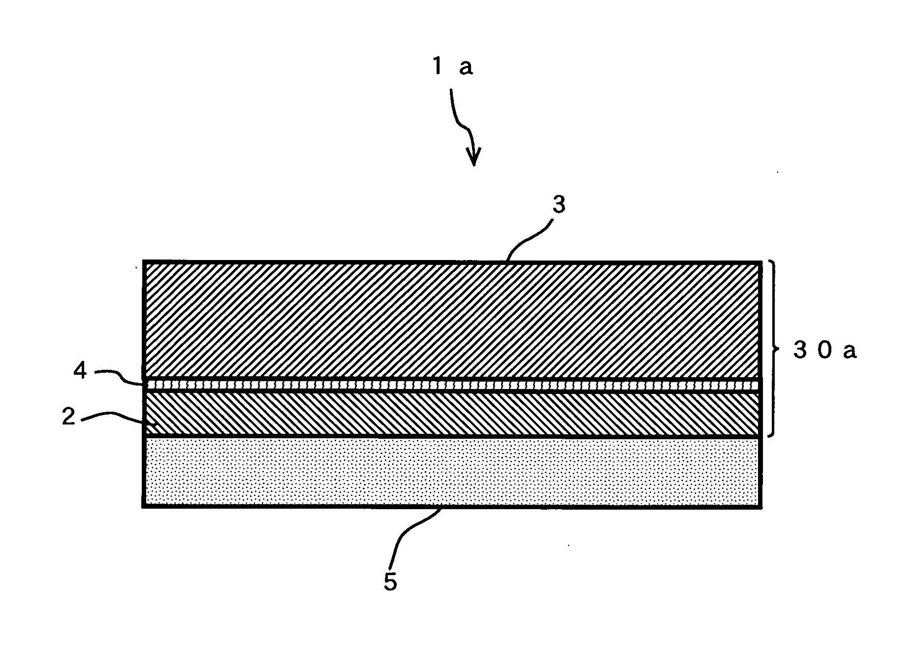
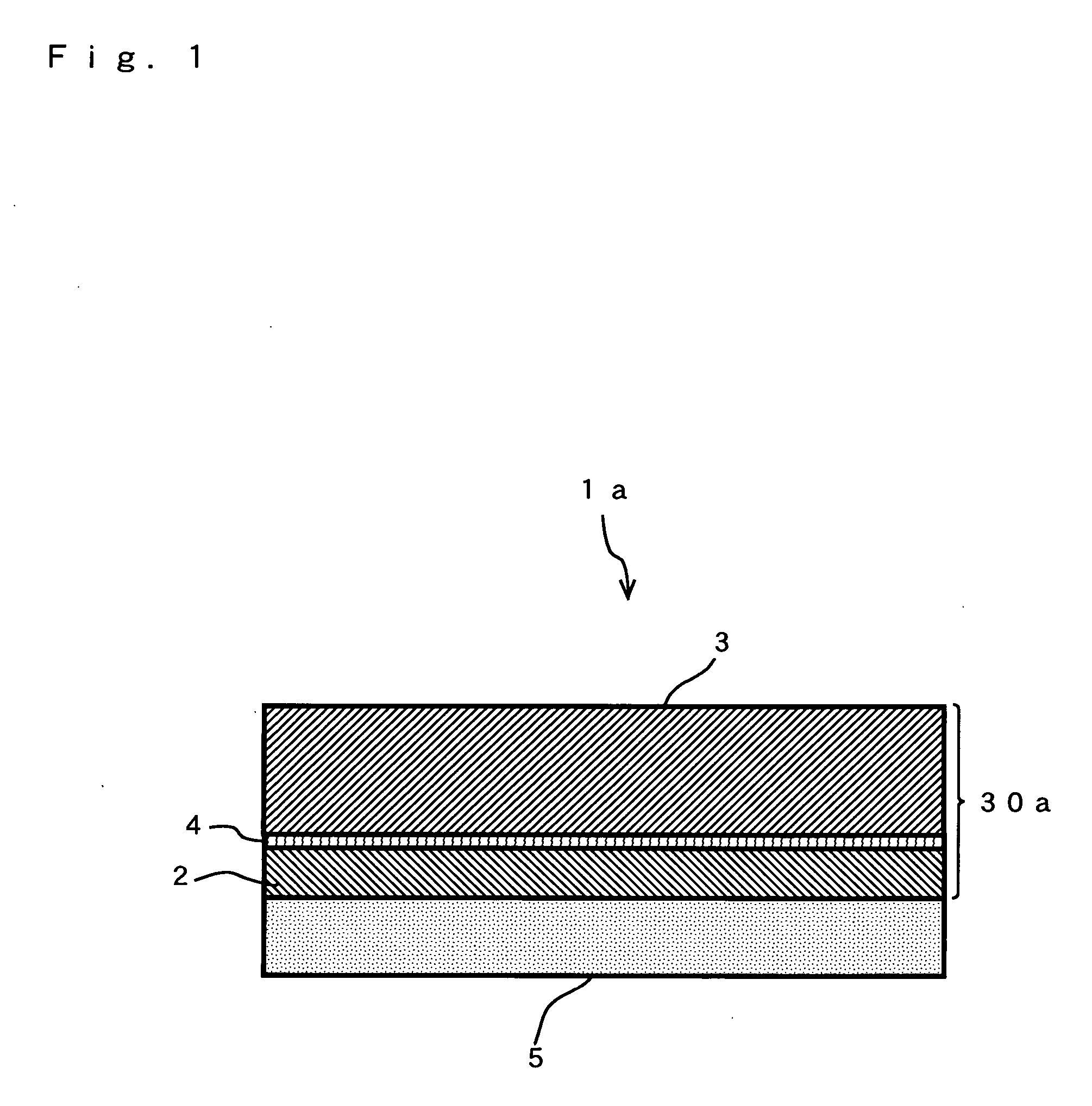
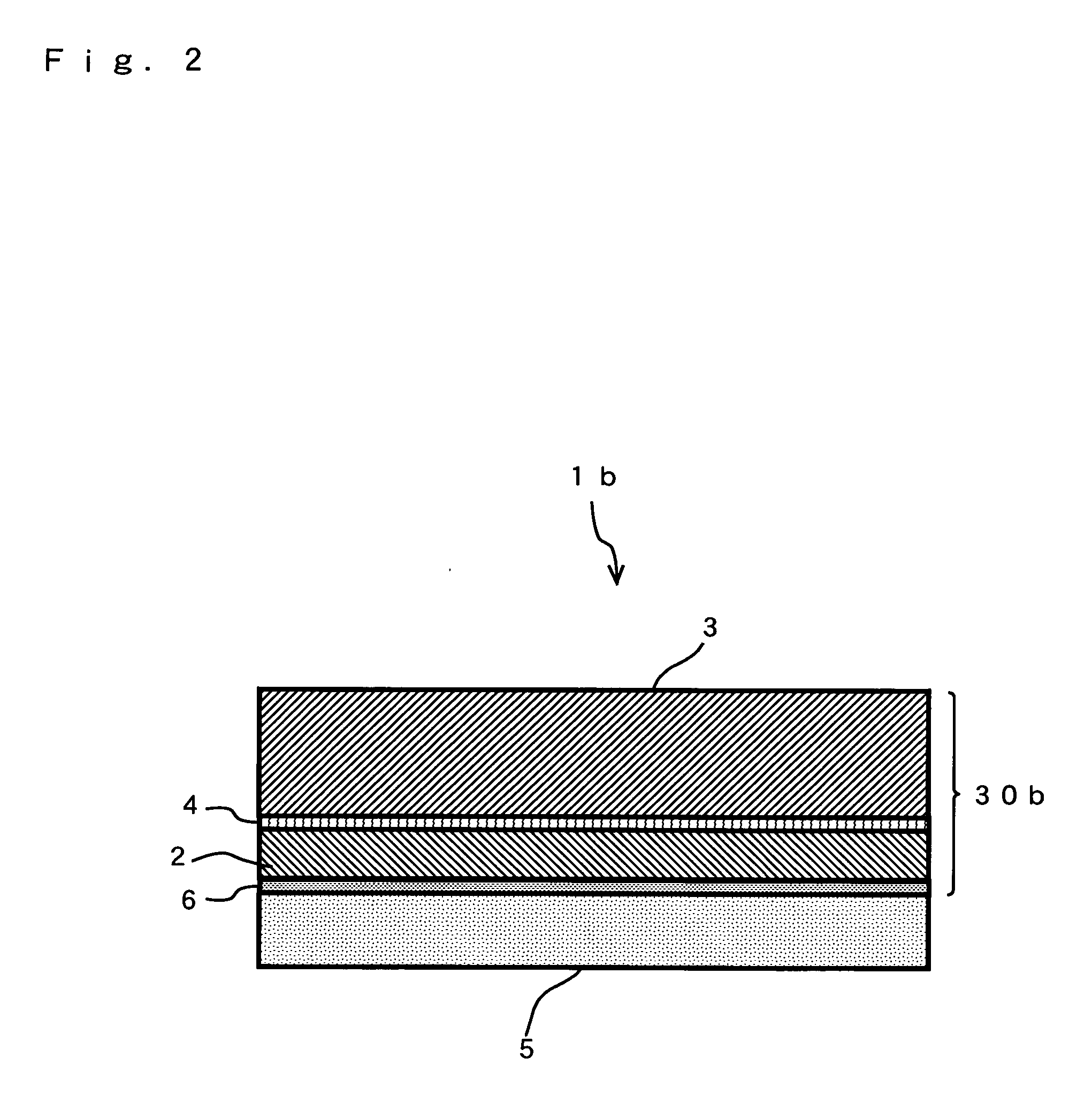
The present invention discloses a technology for a printed wiring board which uses a copper foil without roughening treatment. Therefore, electrodeposited copper foil with carrier foil which is sequentially constituted with carrier foil, bonding interface layer, electrodeposited copper foil with smooth surface on both side and a resin layer is employed. The resin composition constituting the resin layer is composed of 20 to 80 parts by weight of an epoxy resin which includes curing agent, 20 to 80 parts by weight of a solvent soluble aromatic polyamide resin polymer and curing accelerator in a suitable amount if required.

Description

TECHNICAL FIELD [0001] The invention relates to an electrodeposited copper foil with carrier foil on which resin layer for forming an insulating layer is formed, a copper-clad laminate and a printed wiring board obtained by using an electrodeposited copper foil with carrier foil on which resin layer for forming an insulating layer is formed, and a manufacturing method of a multilayer printed wiring board using an electrodeposited copper foil with carrier foil on which resin layer for forming an insulating layer is formed. BACKGROUND ART [0002] Conventional copper foils having been used for manufacturing of printed wiring boards, as disclosed in many documents including Patent Document 1, are subjected to a roughening treatment to make one surface uneven by adhering fine copper particles or by other means. When it is laminated with a base resin such as a prepreg, the unevenness shape of roughened surface of the copper foil buried in the base resin works as anchor effect, whereby the ...

Claims


Application Information

Patent Timeline
Patent Type & Authority Applications(United States)
IPC IPC(8): B32B15/08B32B15/088B32B15/092H05K1/09H05K1/03H05K3/00H05K3/02H05K3/42H05K3/46
CPCH05K3/025H05K3/384H05K3/389H05K3/427H05K3/4652H05K3/4655Y10S428/901Y10T428/12431Y10T428/12903Y10T428/12438Y10T428/12569Y10T428/1291H05K2201/0358B32B15/088B32B15/092B32B15/20B32B27/20B32B2255/06B32B2255/24B32B2457/08
Inventor NAGATANI, SEIJI
Owner MITSUI MINING & SMELTING CO LTD
Learn More