
Organic electroluminescent device

a technology of electroluminescent devices and organic el, which is applied in the direction of discharge tube luminescnet screens, organic chemistry, transportation and packaging, etc., can solve the problems of low power conversion efficiency (w/w), difficult to achieve the required practical operation life-time (10,000 hours or more), and achieves long operational life time, high luminance, and effective and stable device provision

Active Publication Date: 2007-08-09
ROHM CO LTD +2
View PDF3 Cites 187 Cited by
  • Summary
  • Abstract
  • Description
  • Claims
  • Application Information

AI Technical Summary

Benefits of technology

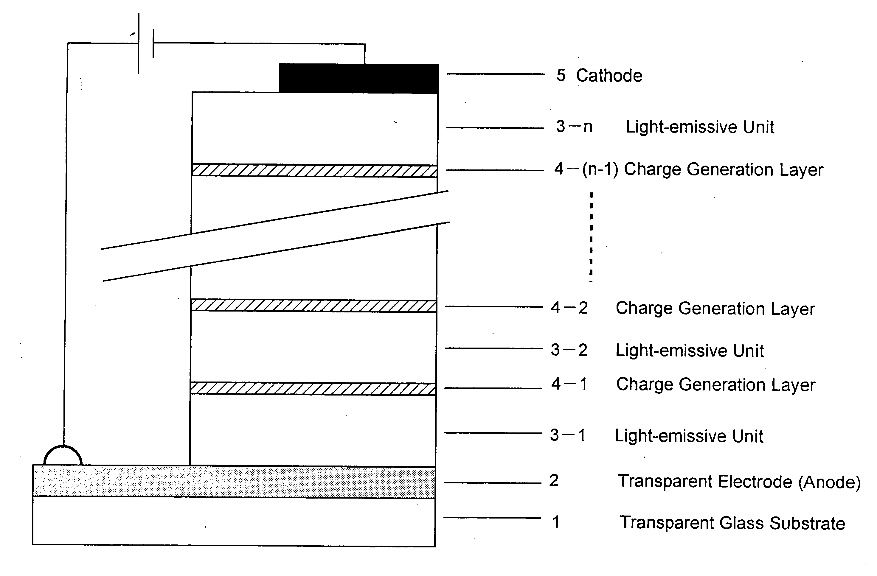
[0025] In view of the above problems in the conventional organic electroluminescent (EL) devices, the present invention provides an organic EL device which can effectively and stably provide a device structure capable of achieving a long operational life time with a light-emission at a higher luminance, which cannot be easily attained in conventional EL devices. In the production of such organic electroluminescent (EL) devices, the formation of two or more light-emissive units (mainly formed from an organic material), sandwiched between a cathode and an anode, frequent change and precise positioning of shadow masks for defining a deposition area is not required during the formation of a charge generation layer, which is newly introduced in the present invention. A formation of the interlayer insulation film in a sudden-changed shape which has a risk of causing disconnection of a cathode line is also not required, thus enabling to enhance productivity and to simplify the process of manufacturing simple matrix-type display devices, etc. According to an aspect of the present invention, an organic electroluminescent device is provided, including at least two light-emissive units provided between a cathode electrode and an anode electrode opposed to the cathode electrode, each of the light-emissive units including at least one light-emissive layer. The light-emissive units are partitioned from each other by at least one charge generation layer, the charge generation layer constituting an electrically insulating layer having a resistivity of not less than 1.0×10² Ωcm.
[0059] It is desirable for light to be able to be passed in only one direction which is one of an anode electrode direction and a cathode electrode direction, from a light generation site in the organic electroluminescent device, wherein light advancing in a direction opposite to the only one direction is absorbed by a light-absorbing medium, and wherein, in each of the light-emissive units, a light interference effect is removed so that an adjustment of an optical path length from a light-emissive site of the light-emissive layers to a light-reflective metal electrode is substantially not necessary.
[0060] It is desirable for light advancing in one direction which is one of an anode electrode direction and a cathode electrode direction, from a light generation site in the organic electroluminescent device to be reflected diffusely by a diffused reflection medium, and in each of the light-emissive units, a light interference effect to be removed, so that an adjustment of an optical path length from a light-emissive site of the light-emissive layers to a light-reflective metal electrode is substantially not necessary.

Problems solved by technology

Namely, Helfrich et al. have observed that an external quantum efficiency of about 5% can be obtained when a sufficient electric field electroluminescence (EL) is applied to an anthracene single crystal; however, according to their method, only a low power conversion efficiency (w / w) could be obtained, since the voltage required to drive such devices is quite high (greater than 100V).
However, from a viewpoint of durability of the device, the above-described conventional organic EL devices can barely attain a half-decay life time exceeding 10,000 hours with a luminance of only the order of 100 cd / m2, which is required in display use.
Presently, it is still difficult to attain a required practical operational life-time (10,000 hours or more) with a luminance of about 1,000 to 10,000 cd / m2, which is required in illumination use, etc.
In fact, an organic EL device having a high luminance and long operational life-time is still not realized and not commercially available.
However, the resulting device still suffers from the disadvantage that if the device is intended to obtain a high luminance emission necessary for illumination purposes, a higher current density approaching tens of mA / cm2 to hundreds of mA / cm2 is necessary.
It can be considered that this property is characteristic of charge injection type devices (like this organic EL device), and such characteristics can cause a relatively large problem with the operational life-time of organic EL devices in comparison with an inorganic LED (light-emitting diode) which is also a charge injection device and uses an inorganic compound semiconductor which can be more robust than organic compounds.
This EL device, however, suffers from the following problem.
In this alternative case, however, a problem of the throughput reduction cannot be also avoided, because a metal such as Al (aluminum), which is a conventional and low-cost wiring material, cannot be used as a cathode material and also it is necessary to stably form “an interlayer insulation film having a layer thickness above 1 μm and a suddenly-changed shape of the inter layer”.
However, as in the above-discussed Japanese Laid-open Patent Application No. 11-329748, if the two or more light-emitting units are separated using a material having a high electrical conductivity (low resistivity) described above, there may be difficulties in defining light emission areas as required, due to the conductivity in a planar (lateral) direction (direction parallel to a substrate).
However, in this method, it is difficult to attain selective emission only in the desired pixels in the display device, because the display device has to be produced at a pixel length and pitch (between each pixel) of about 0.1 mm or less.
In regard to improving productivity in mass-production of the EL devices, frequent changing and precise positioning operations of the shadow mask is not desirable, because it causes tremendous reduction of throughput.

Method used


Image

  • Organic electroluminescent device
  • Organic electroluminescent device
  • Organic electroluminescent device

Examples


reference example 1

(Example for the Production of the Conventional Organic EL Device-Green Light-Emitting Device)

[0204] The conventional organic EL device having a laminate structure shown in FIG. 9 was produced as follows.

[0205] A glass substrate 1 used herein includes, coated in the predetermined pattern on a surface thereof, a transparent anode electrode 2 including an ITO (indium-tin oxide, sputtered product commercially available from ASAHI GLASS, or ion plating product commercially available from Nippon Sheet Glass Co., Ltd.) having a sheet resistance of about 20 Ω / □ (Ω / sq.) (see, FIG. 10A). Alpha (α)—NPD having a hole transporting property was deposited, through a metal mask (shadow mask) 40 for organic layer formation (see FIG. 10B), onto the ITO-coated glass substrate 1 under vacuum of about 10−6 Torr and at a deposition rate of about 2 Å / sec to form a hole transportation layer 6 having a thickness of about 700 Å.

[0206] An organic-metal complex of tris(8-quinolinolato) aluminum (hereinaft...

reference example 2

(Example for the Production of the Conventional Organic EL Device-Blue Light-Emitting Device)

[0213] A conventional organic EL device having a laminate structure shown in FIG. 11 was produced in accordance with the manner similar to Reference Example 1 as follows.

[0214] A glass substrate 1 used herein includes, coated in the predetermined pattern on a surface thereof, a transparent anode electrode 2 including an ITO (indium-tin oxide, sputtered product commercially available from ASAHI GLASS) having a sheet resistance of about 20 Ω / □ (see, FIG. 10A). Spiro-NPB having a hole transporting property was deposited, through a metal mask 40 for organic layer formation (see, FIG. 10B), onto the ITO-coated glass substrate 1 under vacuum of about 10−6 Torr and at a deposition rate of about 2 Å / sec to form a hole transportation layer 9 having a thickness of about 800 Å.

[0215] Spiro-DPVBi represented by the following formula:

was deposited onto the hole transportation layer 9 under vacuum ...

reference example 3

(Example for the Production of the Conventional Organic EL Device-Red Light-Emitting Device)

[0221] A conventional organic EL device having a laminate structure shown in FIG. 12 was produced in a manner similar to Reference Example 1 as follows.

[0222] A glass substrate 1 used herein includes, coated in the predetermined pattern on a surface thereof, a transparent anode electrode 2 including an ITO (indium-tin oxide, sputtered product commercially available from ASAHI GLASS) having a sheet resistance of about 20 Ω / □ (see, FIG. 10A). α-NPD having a hole transporting property was deposited, through a metal mask 40 for organic layer formation (see, FIG. 10B), onto the ITO-coated glass substrate 1 under vacuum of about 10−6 Torr and at a deposition rate of about 2 Å / sec to form a hole transportation layer 12 having a thickness of about 700 Å.

[0223] Alq and a red light-emissive fluorescent dye, “DCJTB” (trade name) commercially available from KODAK, were deposited onto the hole transpo...


PUM

PropertyMeasurementUnit
Angleaaaaaaaaaa
Nanoscale particle sizeaaaaaaaaaa
Electrical resistivityaaaaaaaaaa

Abstract

An organic electroluminescent device includes at least two light-emissive units provided between a cathode electrode and an anode electrode opposed to the cathode electrode, each of the light-emissive units including at least one light-emissive layer. The light-emissive units are partitioned from each other by at least one charge generation layer, the charge generation layer being an electrically insulating layer having a resistivity of not less than 1.0×10² Ωcm.

Description

BACKGROUND OF THE INVENTION [0001] 1. Field of the Invention [0002] The present invention relates to an organic electroluminescent device (hereinafter, abbreviated as an “organic EL device” or “device”) which can be used in planar light sources and display devices. [0003] 2. Description of the Related Art [0004] Recently, attention has been drawn to organic electroluminescent devices having a light-emitting or luminescent layer including an organic compound between a cathode electrode and an anode electrode opposed to the cathode electrode as a large area display device operable at a low driving voltage. For the purpose of higher efficiency in an EL device, Tang et al., as is disclosed in Appl. Phys. Lett., 51, 913 (1987), have successfully achieved a sufficiently high luminance and high efficiency for practice use, i.e., a luminance of 1,000 cd / m2 and an external quantum efficiency of 1% at an applied voltage no more (greater) than 10 volts, by adopting a structure in which organic...

Claims


Application Information

Patent Timeline
IPC IPC(8): H01J1/62H01J63/04C07C211/58C07C211/61C09K11/06H01L51/50H01L51/52H01L51/56H05B33/10H05B33/24
CPCC07C211/58Y10T428/24942C07C2103/18C09K11/06C09K2211/1003C09K2211/1007C09K2211/1011C09K2211/1014H01L51/5036H01L51/5088H01L51/5262H01L51/5278H01L51/56H01L51/5044C07C211/61C07C2603/18H10K50/125H10K50/17H10K50/19H10K50/171H10K59/875H10K71/40H05B33/22H10K50/15H10K50/16H10K50/81H10K50/82H10K50/131H10K50/865H10K50/85H10K71/00H10K85/60H10K85/624H10K85/626H10K85/633
Inventor KIDO, JUNJIHAYASHI, TAKESHI
Owner ROHM CO LTD
Learn More