Driver circuit usable for display panel
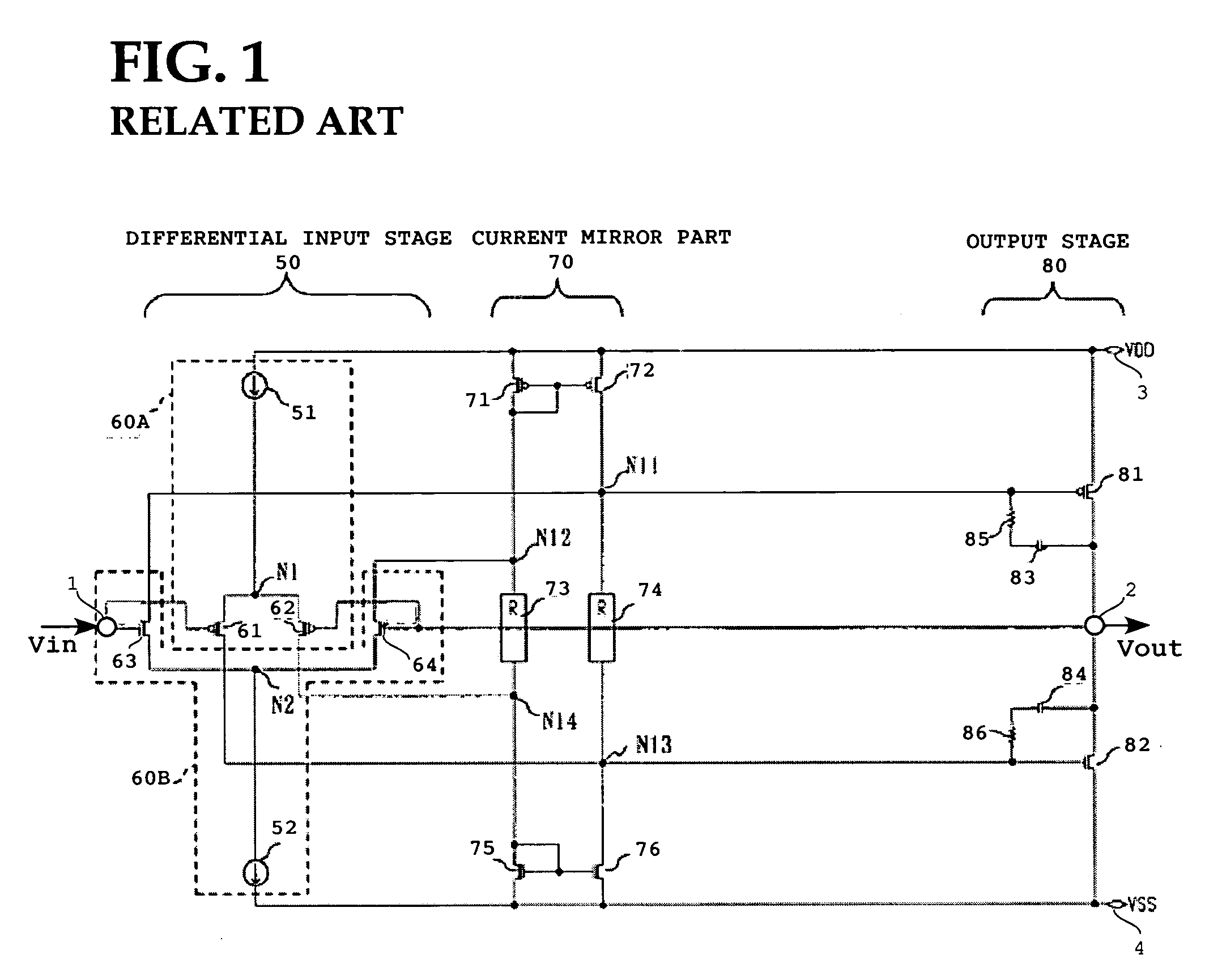
a driver circuit and display panel technology, applied in pulse manipulation, instruments, pulse technique, etc., can solve the problems of increasing the overall consumption of an integrated circuit chip which is integrated with a plurality of driver circuits, and it is difficult to realize a driver circuit usable for a display panel
- Summary
- Abstract
- Description
- Claims
- Application Information
AI Technical Summary
Benefits of technology
Problems solved by technology
Method used
Image
Examples
first embodiment
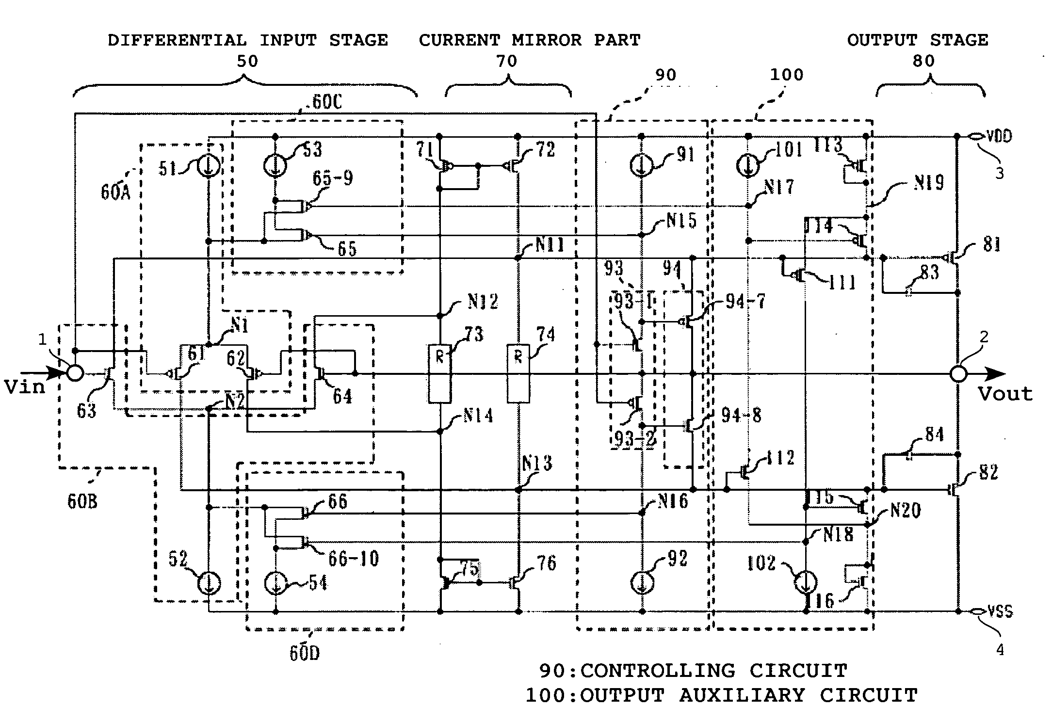
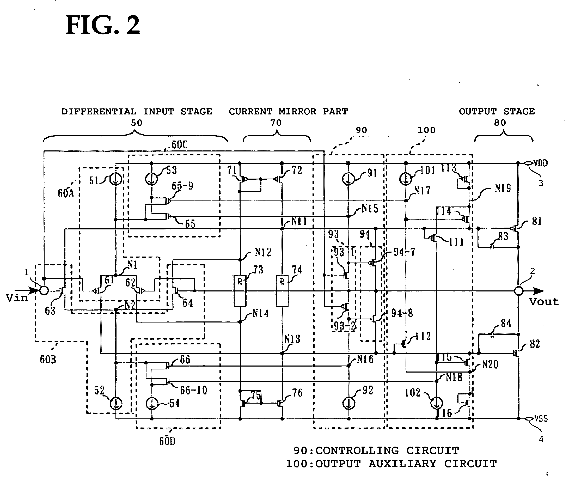
[0032]FIG. 2 is a circuit diagram showing a driver circuit that is a first embodiment of the present invention.
[0033]This driver circuit operational at a high slew rate includes a differential input stage 50, a current mirror part 70, a push-pull type output stage 80, a first auxiliary current source part 60C, a second auxiliary current source part 60D, a controlling circuit 90, and a power output auxiliary circuit 100. The differential input stage 50 has a first differential input stage 60A which is a first conductive type (e.g., a p-type differential input stage) and a second differential input stage which is a second conduction type (e.g., an N-type differential input stage).
[0034]The p-type differential input stage 60A has a first current source 51, a first transistor (e.g., a PMOS transistor) 61, and a second transistor (e.g., a PMOS transistor) 62. The first current source 51 is connected to a power-supply terminal 3 from which a power-supply voltage of VDD level is supplied a...
second embodiment
[0065]FIG. 4 is circuit diagram showing a driver circuit that is a second embodiment of the present invention. Components in FIG. 4 which operate in the same manner as those in FIG. 2 are denoted by the same reference numerals.
[0066]In the driver circuit of the second embodiment, a P-type output stop part 120 and an N-type output stop part 130 are added to the first embodiment.
[0067]The output stop parts 120 and 130 are so configured that electrical potentials at nodes N11 and N13 are fixed on the basis of complementary control signals DSB (e.g., VDD) and XDSB (e.g., VSS). The output stop parts 120 and 130 are also so configured that a PMOS transistor 81 and an NMOS transistor 82 of an output stage 80 are turned off at the same time.
[0068]The P-type output stop part 120 has PMOS transistors 121, 122, 123, and 124 whose gate are controlled by the control signal DSB and a PMOS transistor 125 whose gate is controlled by the control signal XDSB having a reversed phase. Source and drain ...
third embodiment
[0075]FIG. 5 is a circuit diagram showing a driver circuit that is a fourth embodiment of the present invention. Components in FIG. 5 which operate in the same manner as those in FIG. 2 are denoted by the same reference numerals.
[0076]In the driver circuit of the third embodiment, the PMOS transistor 65-9 and the NMOS transistor 66-10 are deleted from the first auxiliary current source part 60C and the second auxiliary current source part 60D, respectively, both of which are included by the driver circuit of the first embodiment. The output auxiliary circuit 100 for controlling gated of the PMOS transistor 65-9 and the NMOS transistor 66-10 are also the output auxiliary circuit 100 of the first embodiment Other components are similar to those of the first embodiment.
[0077]The driver circuit of the third embodiment sequentially performs operations (1), (2), (3), and (5) which are described in the first embodiment and performs to a regular operation.
[0078]FIG. 3 is the wave form chart...
PUM
 Abstract
Description
Claims
Application Information
 - R&D
- Intellectual Property
- Life Sciences
- Materials
- Tech Scout
- Unparalleled Data Quality
- Higher Quality Content
- 60% Fewer Hallucinations
Browse by: Latest US Patents, China's latest patents, Technical Efficacy Thesaurus, Application Domain, Technology Topic, Popular Technical Reports.
© 2025 PatSnap. All rights reserved.Legal|Privacy policy|Modern Slavery Act Transparency Statement|Sitemap|About US| Contact US: help@patsnap.com


