Nitrogen-doped silicon substantially free of oxidation induced stacking faults

a technology of nitrogen-doped silicon and stacking faults, which is applied in the direction of polycrystalline material growth, crystal growth process, growth of polycrystalline materials, etc., can solve the problems of affecting the electronic properties of the wafer, affecting the yield potential of the material, and the number of defects in single crystal silicon form

Inactive Publication Date: 2007-07-26
GLOBALWAFERS CO LTD
View PDF8 Cites 17 Cited by
  • Summary
  • Abstract
  • Description
  • Claims
  • Application Information

AI Technical Summary

Benefits of technology

[0012] Among the objects and features of the present invention, therefore, is the provision of an epitaxial silicon wafer wherein the epitaxial layer is substantially free of defects associated with oxidation induced stacking faults; the provision of such a wafer wherein the substrate is doped with nitrogen; the provision of such a substrate wafer wherein vacancies are the predominant intrinsic point defect; and, the provision of such a substrate wafer which is substantially free of oxidation induced stacking faults. Further among the objects and features of the present invention is the provision of a process for preparing a single crystal silicon ingot, from which such a substrate wafer is obtained.

Problems solved by technology

It is now recognized that a number of defects in single crystal silicon form in the crystal growth chamber as the crystal cools after solidification.
Agglomerated intrinsic point defects in silicon can severely impact the yield potential of the material in the production of complex and highly integrated circuits.
Such defects are not responsible for gate oxide integrity failures, an important wafer performance criterion, but they are widely recognized to be the cause of other types of device failures usually associated with current leakage problems.
Without the ability to getter metallic impurities, the electronic properties of the wafer may be negatively impacted; for example, the wafer may have a decreased minority carrier lifetime, current leakage at p-n junctions, dielectric constant discontinuity and reduced breakdown strength.
This method decreases throughput and significantly increases the cost of manufacturing the silicon wafers.
However, the high gettering capability was due in part to the nearly uniform distribution of OISF throughout the wafer which negatively impacts the quality of the epitaxial wafer.
OISF continue to grow through the epitaxial layer and result in grown-in defects commonly referred to as epitaxial stacking faults.

Method used


Image

  • Nitrogen-doped silicon substantially free of oxidation induced stacking faults
  • Nitrogen-doped silicon substantially free of oxidation induced stacking faults
  • Nitrogen-doped silicon substantially free of oxidation induced stacking faults

Examples


example 1

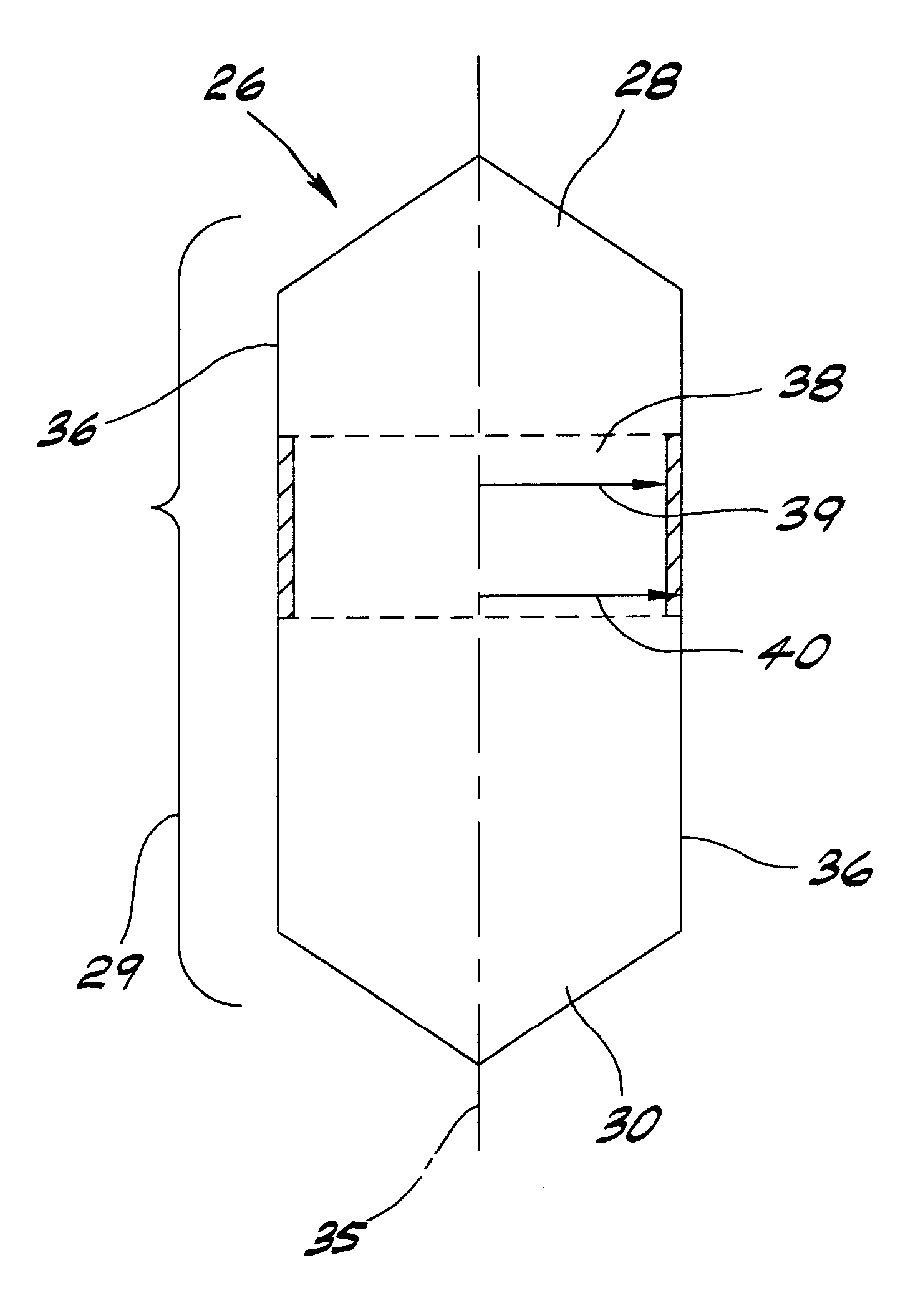
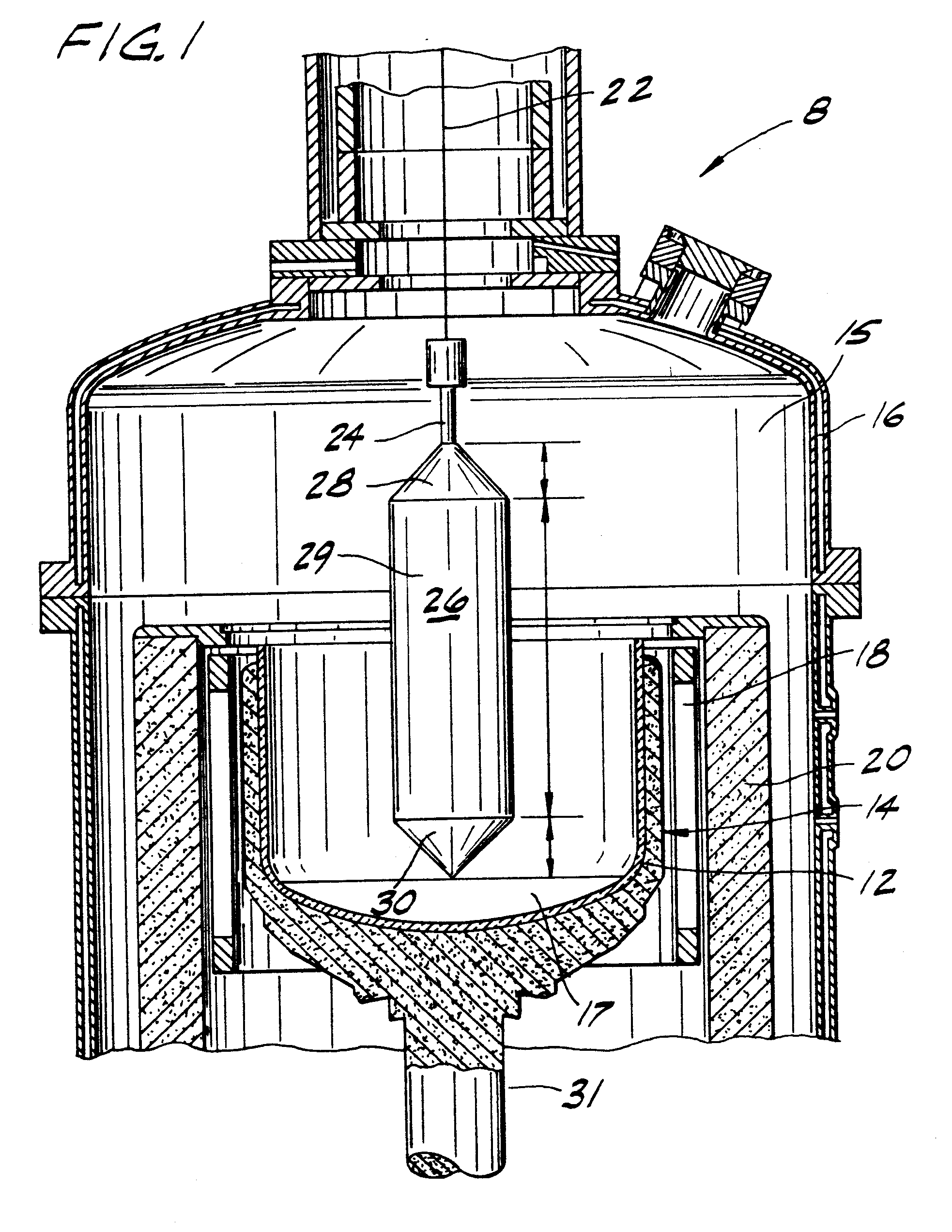
[0058] A p−-type single crystal ingot having a diameter of 200 mm and {100} crystallographic orientation was pulled from a 24 inch crucible containing about 140 kg of polysilicon and about 320 mg of silicon nitride. The pulling rate was about 1.0 mm / min. The crucible rotation rate was controlled to between about 5 rpm near the seed end of the ingot to about 8 rpm near the tail end of the ingot to yield an oxygen concentration of about 13±0.5 ppma at the center of the crystal (Oic). The crystal rotation rate was about 6 rpm and the oxygen concentration over the length of the constant diameter portion at 6 mm from the edge was between about 10.4 ppma to about 9.3 ppma. The radial gradient of oxygen concentration distribution was about 20% to about 40%. The target nitrogen concentration at the top of the ingot was about 6×10¹³ atoms / cm3. The target nitrogen concentration at the bottom of the ingot was about 22×1013 atoms / cm3. Due to the very low distribution coefficient of nitrogen in ...

example 2

[0067] A p−-type single crystal ingot of having a diameter of 300 mm and orientation {100} was pulled from a 32 inch crucible containing about 250 kg of polysilicon and about 600 mg of silicon nitride. The pulling rate was about 0.7 mm / min. The crucible rotation rate was controlled between about 4.5 rpm and about 6.5 rpm to yield an oxygen concentration of about 12.5±0.5 ppma at the center of the crystal. The crystal rotation rate was about 4 rpm and the oxygen concentration over the length of the constant diameter portion at 6 mm from the edge was between about 9.0 ppma to about 7.5 ppma. The radial gradient of oxygen concentration distribution was about 20% to about 40%. The target nitrogen concentration at the top of the ingot was 6×10¹³ atoms / cm3. The target nitrogen concentration at the bottom of the ingot was 15×1013 atoms / cm3.

[0068] The ingot was sliced into wafers which were polished to a specular gloss and a 2.5 μm thick epitaxial layer was deposited on the front surface o...


PUM

PropertyMeasurementUnit
temperatureaaaaaaaaaa
diameteraaaaaaaaaa
diametersaaaaaaaaaa

Abstract

The present invention relates to a process for forming single crystal silicon ingots or wafers that contain an axially symmetric region in which vacancies are the predominant intrinsic point defect, that are substantially free of oxidation induced stacking faults, and are nitrogen doped to stabilize oxygen precipitation nuclei therein.

Description

CROSS-REFERENCE TO RELATED APPLICATIONS [0001] This application is a divisional of U.S. patent application Ser. No. 10 / 380,806 filed on Mar. 18, 2003, which claims priority from PCT application Serial No. PCT / US01 / 27049 filed on Aug. 30, 2001, which claims priority from U.S. provisional application Ser. No. 60 / 308,521 filed on Jul. 27, 2001, which claims priority from Japanese application Serial No. 2000-283033 filed on Sep. 19, 2000, the entire disclosures which are incorporated herein by reference.BACKGROUND OF THE INVENTION [0002] The present invention relates generally to the preparation of semiconductor grade single crystal silicon which is used in the manufacture of electronic components. More particularly, the present invention relates to vacancy dominated single crystal silicon ingots and wafers that are doped with nitrogen to stabilize oxygen precipitation nuclei and are substantially free of oxidation induced stacking faults. [0003] Single crystal silicon, from which a sin...

Claims


Application Information

Patent Timeline
Patent Type & Authority Applications(United States)
IPC IPC(8): C30B15/00C30B21/06C30B27/02C30B19/00
CPCC30B15/203C30B29/06C30B15/206
Inventor HAGA, HIROYOAOSHIMA, TAKAAKIBANAN, MOHSEN
Owner GLOBALWAFERS CO LTD
Why Eureka
Try Eureka