
Heterojunction bipolar transistor and method for manufacturing same

a technology of heterojunction and transistor, applied in the direction of transistor, electrical apparatus, semiconductor devices, etc., can solve the problems of unfavorable product safety, unfavorable product safety, and complex manufacturing process, and achieve the effect of preventing high silicide resistance resulting from ge atoms, high manufacturing cost, and high transistor performan

Inactive Publication Date: 2007-04-19
PANASONIC CORP
View PDF6 Cites 14 Cited by
  • Summary
  • Abstract
  • Description
  • Claims
  • Application Information

AI Technical Summary

Benefits of technology

[0018] The Ge composition profile of the layer structure corresponding to the intrinsic base region 106 is optimized to improve device property. For example, the Si graded base layer 111 has the graded composition base structure in which Ge content gradually increases from the emitter to the collector. Thereby, an electric field is formed inside the base layer, which accelerates the carrier (electron) so as to decrease electron transit time for the base layer, and then high frequency property (high speed of the device) is obtained.
[0043] With this manufacturing method, the second silicon-germanium layer comprising silicon and germanium is formed by a vapor phase growth based on reactant gas of chlorine addition; thereby growth of the extrinsic base formation layer is suppressed under etching function of the reactant gas containing chlorine. As a result, germanium content of the second silicon-germanium layer can be made lower than that of the first silicon-germanium layer. And, when forming the silicide layer on the third silicon layer covering the second silicon-germanium layer, it is ensured that silicidation is not affected by Ge atom so as to prevent increase of silicide resistance.

Problems solved by technology

Thereby, the SiGeHBT of the double-polysilicon structure increases contact resistance between the polysilicon layer 103 and the epitaxial SiGe layer 104 and it causes a problem that uneven contact resistance exists among products.
And it has further problems that manufacturing process is complicated and process window is small during selective growth.
From these viewpoints, the SiGeHBT of the double-polysilicon structure is not suitable for mass production.

Method used


Image

  • Heterojunction bipolar transistor and method for manufacturing same
  • Heterojunction bipolar transistor and method for manufacturing same
  • Heterojunction bipolar transistor and method for manufacturing same

Examples


first embodiment

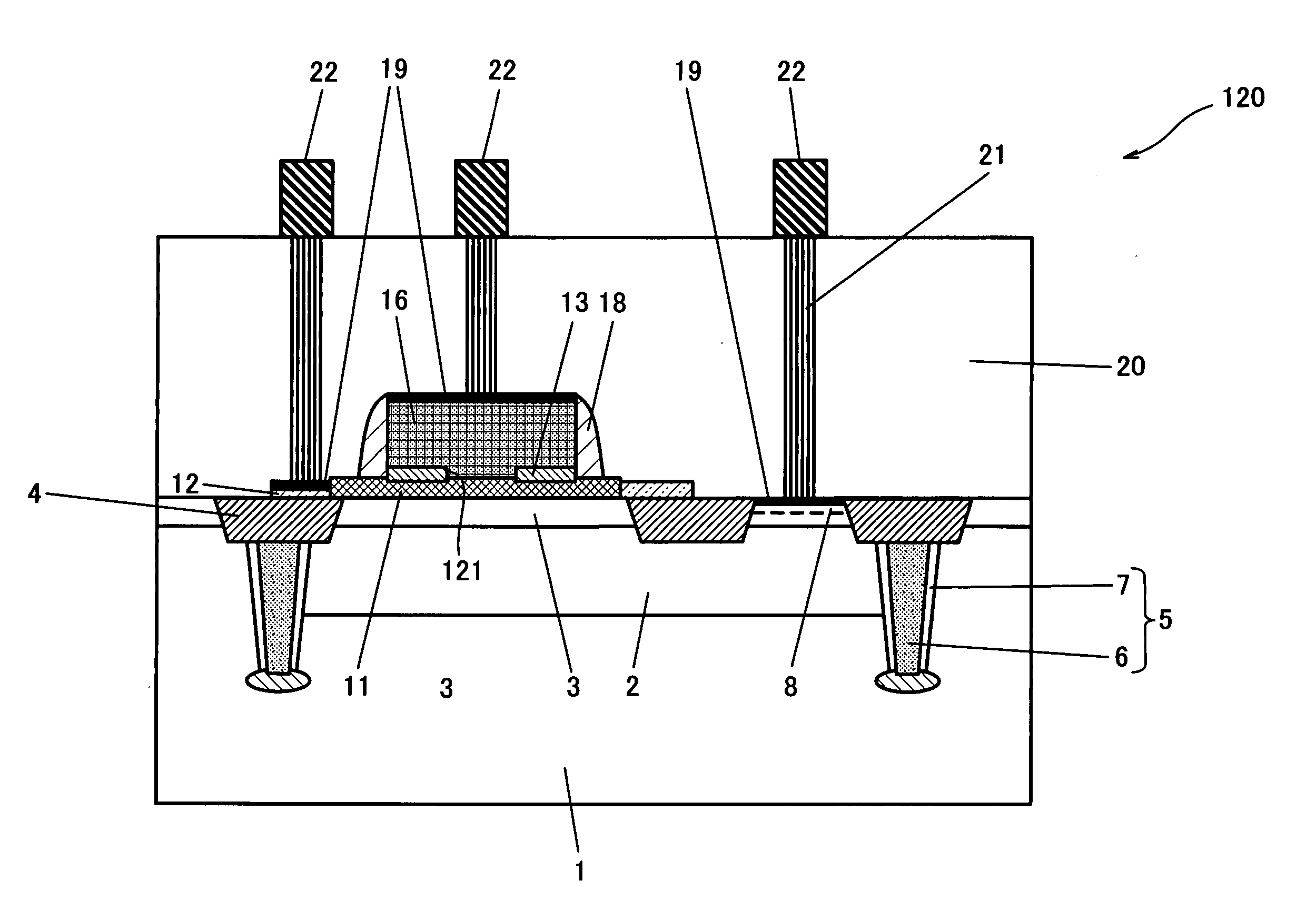
[0074]FIG. 1 is a sectional view showing a configuration of SiGe HBT of a first embodiment in the present invention.

[0075] As shown in FIG. 1, arsenic ions are implanted into a surface of a P-type Si substrate 1 to form an N-type subcollector region 2 having appropriately 1 μm depth. A Si monocrystal layer 3 having 0.5 μm thickness epitaxially grows on the Si substrate 1 and the subcollector region 2 while doping an N-type impurity so as to covers the substrate 1 and the subcollector region 2.

[0076] A shallow trench 4 buried with a silicon oxide layer is formed so as to extend from a surface of the Si monocrystal layer 3 to the Si substrate 1, as an isolation region. And, a deep trench 5 comprising a non-dope polysilicon layer 6 and a silicon oxide layer 7 enclosing the polysilicon layer 6 is extended downward from the shallow trench 4 and formed inside the Si substrate 1.

[0077] A HBT formation region is enclosed with the deep trench 5 and the subcollector region 2 is formed insi...

second embodiment

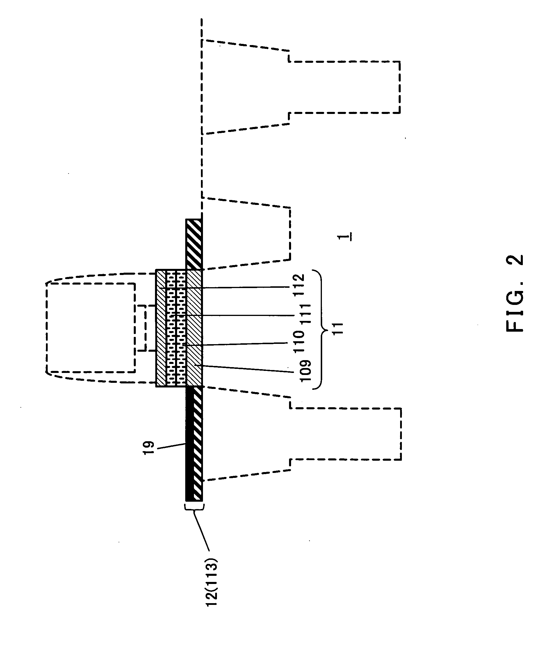
[0139]FIG. 15 is a sectional view showing the SiGe HBT of a second embodiment in the present invention. FIG. 16 is a sectional view showing the base layer (the intrinsic base region 11 and the extrinsic base region 12) of the SiGe HBT. Elements but the extrinsic base region 12 is abbreviated with dot lines.

[0140] Configurations of the SiGe HBT 130 shown in FIG. 15 except for the extrinsic base region 12 are the same with that of the SiGe HBT 120 of the first embodiment (FIG. 1). Therefore, explanations on common configurations are omitted and the extrinsic base region 12 is explained with reference to FIG. 2.

[0141] In FIG. 16, the extrinsic base region 12 comprises the first polycrystal layer 113 as the extrinsic base formation layer, the second polycrystal layer 114 as the extrinsic base formation layer, the third polycrystal layer 115 as the extrinsic base formation layer, the fourth polycrystal layer 116 as the extrinsic base formation layer, and the Co silicide layer 19. These...


PUM


Abstract

A bipolar transistor 120 comprises a substrate 1, a intrinsic base region 11 and an extrinsic base region 12. The intrinsic base region 11 comprises a silicon buffer layer 109 comprised of silicon which is formed on the substrate 1, and a composition-ratio graded base layer 111 which is formed on the silicon buffer layer and comprises silicon and at least germanium and where a composition ratio of the germanium to the silicon varies in a thickness direction of the composition-ratio graded base layer 111. The extrinsic base region 12 comprises an extrinsic base formation layer 113 comprised of silicon which is formed on the substrate and adjacent to the silicon buffer layer. And the thickness of the extrinsic base formation layer 113 is not less than 40 nm.

Description

TECHNICAL FIELD [0001] The present invention relates to a heterojunction bipolar transistor with base layers formed by epitaxial growth and a method for manufacturing the same. BACKGROUND ART [0002] In the field of bipolar transistors, energetically developed are heterojunction bipolar transistors (HBTs) in which materials different in bandwidth are introduced to base layers using epitaxial growth to increase device speed. HBT with base layers using family-IV semiconductor materials such as SiGe (silicon-germanium) material and SiGeC (silicon-germanium carbon) material is highly expected as a high-speed device because the device can be formed on a Si substrate and integration with CMOS circuits and large substrate are advantageous in terms of high performance and low cost. [0003] A typical configuration example of a conventional HBT using SiGe for heterojunction (hereinafter referred as to SiGe HBT) is explained with reference to FIG. 23. While the HBT using SiGe material for base l...

Claims


Application Information

Patent Timeline
IPC IPC(8): H01L27/082H01L21/331H01L29/737
CPCH01L29/66242H01L29/7378
Inventor SAITOH, TOHRUKAWASHIMA, TAKAHIROIDOTA, KENKANZAWA, YOSHIHIKOOHNISHI, TERUHITO
Owner PANASONIC CORP
Learn More