Soldering device and method for forming electrical solder connections in a disk drive unit

a technology of disk drive unit and soldering device, which is applied in the direction of soldering apparatus, metal working apparatus, manufacturing tools, etc., can solve the problems of weak mechanical strength, inability to apply to small slider pads and small pitches, and difficult rework of gbb

Inactive Publication Date: 2007-04-05
SAE MAGNETICS (HK) LTD
View PDF7 Cites 21 Cited by
  • Summary
  • Abstract
  • Description
  • Claims
  • Application Information

AI Technical Summary

Benefits of technology

[0018] Still another aspect of the present invention relates to a bond head for a soldering device that forms electrical solder connections in a disk drive unit. The bond head includes a housing that provides a primary passage structured to receive a solder ball from a solder ball supply. ...

Problems solved by technology

However, GBB is difficult to rework, and cannot be applied to small slider pads and small pitch.
Also, GBB includes ESD issues.
However, USB is sensitive to material with weak mechanical strength, therefore requiring a conformal coating for protection.
ACF is difficult to rework and therefore cannot be used for multi head bonding.
Conventional solder requires significant room for pad layout.
However, manual solder or screw tightening can result in component contamination.
However, manual solder can result in component contamination.
However, conventional solder can result in component contamination, and the male / female connector requires significant room which is unsuitable for micro drives.
Thus, while the conventional methods described above provide an effective solution for connection, they also include several drawbacks.

Method used


Image

  • Soldering device and method for forming electrical solder connections in a disk drive unit
  • Soldering device and method for forming electrical solder connections in a disk drive unit
  • Soldering device and method for forming electrical solder connections in a disk drive unit

Examples


first embodiment

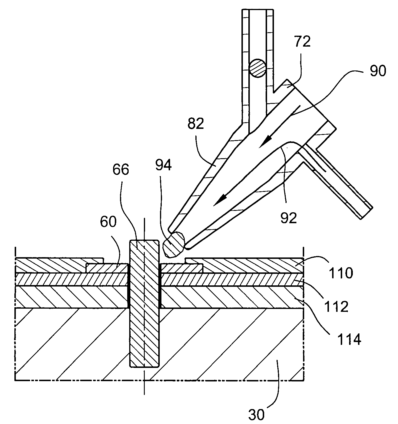
[0074]FIGS. 17-22 illustrate a HGA being electrically connected to a FPC. As shown in FIG. 17, the FPC 36 is initially assembled to the fantail spacer 30 by electrically connecting the voice coil connection pads 58 with voice coil leads 64 and electrically connecting the grounding pin connection pad 60 with the grounding pin 66 as explained above. Then, the HGAs 32 and 34 (with respective sliders 20 connected thereto) are secured by the securing means to the fantail spacer 30, which aligns the suspension pads 56 of the HGAs 32 and 34 with respective FPC pads 62 of the FPC assembly 38. As illustrated, the suspension pads 56 are parallel with respective FPC pads 62 such that the suspension pads 56 cover respective FPC pads 62. Also, the suspension pads 56 of the HGAs 32 and 34 are positioned on opposing sides of the fantail spacer 30 such that soldering occurs on both sides of the fantail spacer 30.

[0075] As shown in FIGS. 18 and 19, each suspension pad 56 includes multiple layers inc...

second embodiment

[0077]FIGS. 23-31 illustrate a HGA being electrically connected to a FPC. As shown in FIG. 23, the HGAs 232 and 234 (with respective sliders 220 connected thereto) are initially aligned with the FPC 236 provided on the fantail spacer 230 such that the suspension pads 256 of the HGAs 232, 234 align with respective FPC pads 262 of the FPC assembly 238 of the FPC 236. As illustrated, the suspension pads 256 are parallel with respective FPC pads 262 such that the suspension pads 256 cover respective FPC pads 262. Also, the suspension pads 256 of the HGAs 232, 234 are positioned on the same side of the fantail spacer 230 such that soldering occurs on a single side of the fantail spacer 230.

[0078] As shown in FIGS. 24 and 25, each suspension pad 256 includes multiple layers including a conductive bonding pad 120, and insulation layers 122, 124 on opposing sides of the bonding pad 120. As illustrated, an opening 126 is provided in the bonding pad 120 to allow connection with a respective F...

third embodiment

[0081]FIGS. 32-34 illustrate a HGA being electrically connected to a FPC. As shown in FIGS. 32 and 33, the suspension base plate 350 of respective HGAs 332, 334 (with respective sliders 320 connected thereto) are initially aligned with the fantail spacer 330, and then coupled thereto by a plurality of securing means, e.g., bearing 342, washer 344, and nut 346. When coupled, the suspension pads 356 of the HGAs 332, 334 align with respective FPC pads 362 of the FPC assembly 338. As best shown in FIGS. 33 and 34, the suspension pads 356 are transverse, e.g., generally perpendicular, with respective FPC pads 362. Also, the suspension pads 356 of the HGAs 332, 334 are adjacent the same side of the fantail spacer 330 such that soldering occurs on a single side of the fantail spacer 330.

[0082] The suspension pads 356 and FPC pads 362 may have any suitable structure, and the suspension pads 356 may be positioned adjacent respective FPC pads 362 in any suitable manner. Also, in the illustrat...


PUM

PropertyMeasurementUnit
Diameteraaaaaaaaaa

Abstract

A soldering device for forming electrical solder connections in a disk drive unit includes a bond head, a laser unit, a pressurized gas supply, and a solder ball supply. The bond head includes a housing that provides a primary passage and two supplemental passages that communicate with the primary passage. The laser unit is operable to direct a laser beam through the primary passage. The pressurized gas supply is operable to deliver pressurized gas through one supplemental passage and into the primary passage. The solder ball supply is operable to deliver a single solder ball through the other supplemental passage and into the primary passage. The primary passage has a tapered configuration structured to maintain a solder ball within the primary passage to allow a laser beam from the laser unit to act upon the solder ball before the solder ball is discharged from the bond head by pressurized gas.

Description

FIELD OF THE INVENTION [0001] The present invention relates to a disk drive unit and, more particularly, to a soldering device and method for forming electrical solder connections in a disk drive unit. BACKGROUND OF THE INVENTION [0002] One known type of information storage device is a disk drive unit that uses magnetic media to store data and a movable read / write head that is positioned over the media to selectively read from or write to the disk. [0003]FIGS. 1-2 illustrate a typical disk drive unit 10 that includes a motor base assembly 12, a top cover 14, and a printed circuit board assembly (PCBA) 16. As illustrated, the motor base assembly 12 includes a head stack assembly (HSA) 18 with slider(s) 20 thereon (see FIG. 3), a magnetic disk 22 mounted on a spindle motor 24 for spinning the disk 22, and a motor base 26 to enclose the above-mentioned components. The slider(s) 20 flies over the surface of the magnetic disk 22 at a high velocity to read data from or write data to the c...

Claims


Application Information

Patent Timeline
IPC IPC(8): B23K26/00
CPCB23K1/0016B23K1/0056B23K3/0623B23K26/123B23K26/14B23K26/1476B23K2201/42H05K3/3442H05K3/3447H05K3/3478H05K3/3494H05K2201/10727H05K2203/0195H05K2203/041H05K2203/081H05K2203/107G11B5/4846G11B5/4853B23K2101/42
Inventor HO, YIUSINGLU, GUOHONG
Owner SAE MAGNETICS (HK) LTD
Why Eureka
Try Eureka