Method for reducing critical dimension and semiconductor etching method

a critical dimension and semiconductor technology, applied in the field of semiconductor etching, can solve the problems of inability to use a further miniaturization device, inability unstable photoresist trimming process, so as to reduce the critical dimension, improve the process stability, and uniformize the critical dimension

Active Publication Date: 2007-03-08
UNITED MICROELECTRONICS CORP
View PDF4 Cites 1 Cited by
  • Summary
  • Abstract
  • Description
  • Claims
  • Application Information

AI Technical Summary

Benefits of technology

[0008] At least on object of the present invention is to provide a method for reducing the critical dimension, wherein th...

Problems solved by technology

Thus, the electrical performance of a MOS transistor will affect the quality of the product.
However, confined by the yellow light process, this approach can not be used for further miniaturization of devices to attain the smallest line width for the gate.
However, the photoresist trimming process is not stable.
When the etching is t...

Method used


Image

  • Method for reducing critical dimension and semiconductor etching method
  • Method for reducing critical dimension and semiconductor etching method
  • Method for reducing critical dimension and semiconductor etching method

Examples


Embodiment Construction

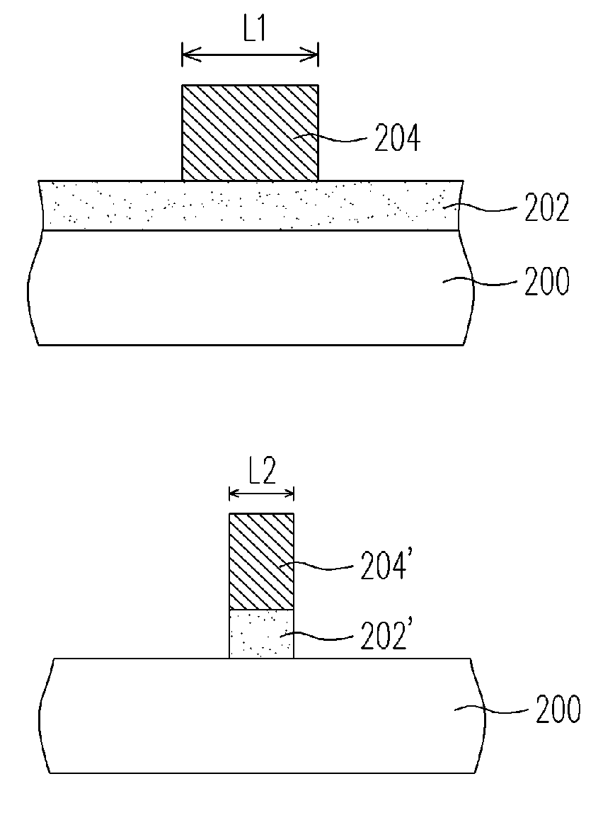
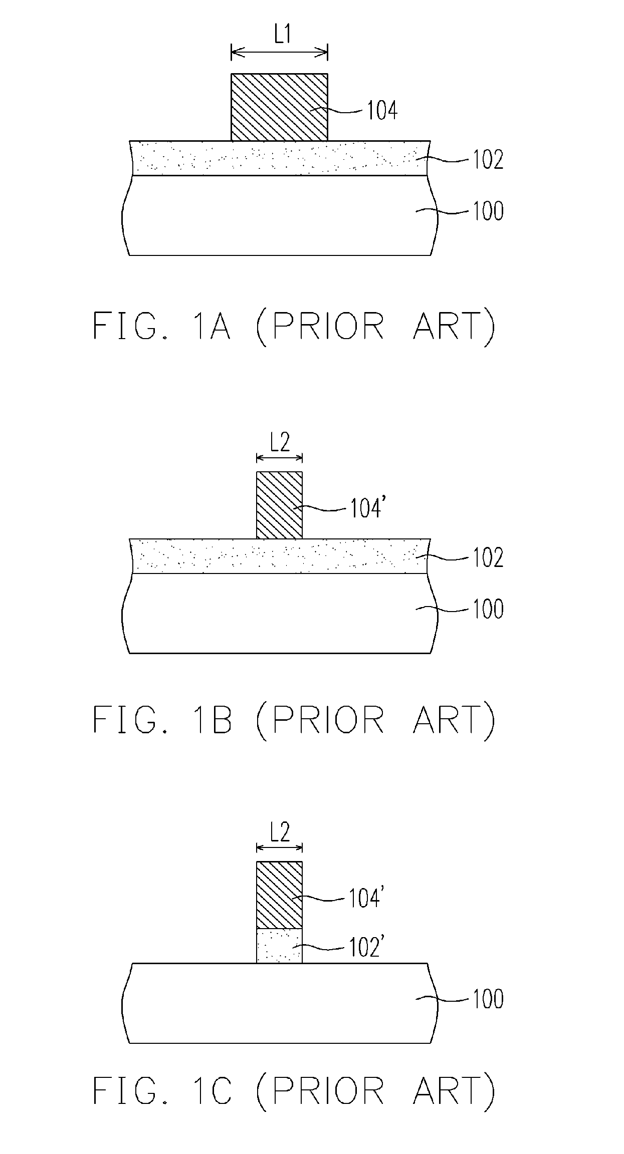
[0029]FIGS. 2A through 2B are schematic cross-sectional views showing the steps of a method for reducing the critical dimension according to one embodiment of the present invention. According to FIG. 2A, a dielectric layer 202 is formed on a substrate 200, wherein the material of the dielectric layer includes, but not limited to, silicon oxide, silicon nitride or silicon oxynitride. A patterned photoresist layer 204 is formed on the dielectric layer 202, wherein the patterned photoresist layer 204 exposes a part of the dielectric layer 202. The patterned photoresist layer 204 further includes a first line width L1.

[0030] Referring to FIG. 2B, using a patterned photoresist layer 204 as an etching mask, an etching is performed under a pressure of about 80 to 400 torrs and at a temperature between −50° C. to 50° C. The exposed dielectric layer 202 is removed, and a downsized patterned photoresist layer 204′ and a patterned dielectric layer 202′ with a final line width L2 less than the...


PUM

PropertyMeasurementUnit
Temperatureaaaaaaaaaa
Pressureaaaaaaaaaa

Abstract

A method of reducing critical dimension is provided. A dielectric layer is formed on a substrate. Then, a patterned photoresist is formed on the dielectric layer to expose part of the dielectric layer, wherein the patterned photoresist has a first line width. An etching process is performed to remove the exposed dielectric layer by using the patterned photoresist as an etching mask, wherein the final line width of the dielectric layer is smaller than the first line width. The conditions of the etching process include an etching pressure at 80 torr to 400 torr, an etching gas that includes a fluorocarbon compound and oxygen, wherein the ratio of the fluorocarbon compound to the oxygen is large than 0 and less than 10. Consequently, the etching process can be stabilized to form a smooth sidewall for the gate and to provide a uniform critical dimension.

Description

BACKGROUND OF THE INVENTION [0001] 1. Field of the Invention [0002] The present invention relates to semiconductor process. More particularly, the present invention relates to a method for reducing the critical dimension (CD) and a semiconductor etching method. [0003] 2. Description of Related Art [0004] The metal-oxide semiconductor (MOS) transistor is an essential electronic element in the integrated circuits. Thus, the electrical performance of a MOS transistor will affect the quality of the product. A general approach in raising the electrical performance of a MOS transistor is to reduce the smallest linewidth of the gate to increase the operation speed of the gate. Normally, during the fabrication of the gate, a hard mask layer is first formed on the polysilicon layer. Further using a patterned photoresist layer above the hard mask layer as an etching mask, an etching process is performed on the hard mask layer. The hard mask layer is then used as a mask for etching the polysil...

Claims


Application Information

Patent Timeline
IPC IPC(8): C23F1/00H01L21/461B44C1/22
CPCH01L21/3088H01L21/32139H01L21/31144H01L21/31116
Inventor TSAI, CHANG-HU
Owner UNITED MICROELECTRONICS CORP
Why Eureka
Try Eureka