Gradient structures interfacing microfluidics and nanofluidics, methods for fabrication and uses thereof
- Summary
- Abstract
- Description
- Claims
- Application Information
AI Technical Summary
Benefits of technology
Problems solved by technology
Method used
Image
Examples
examples
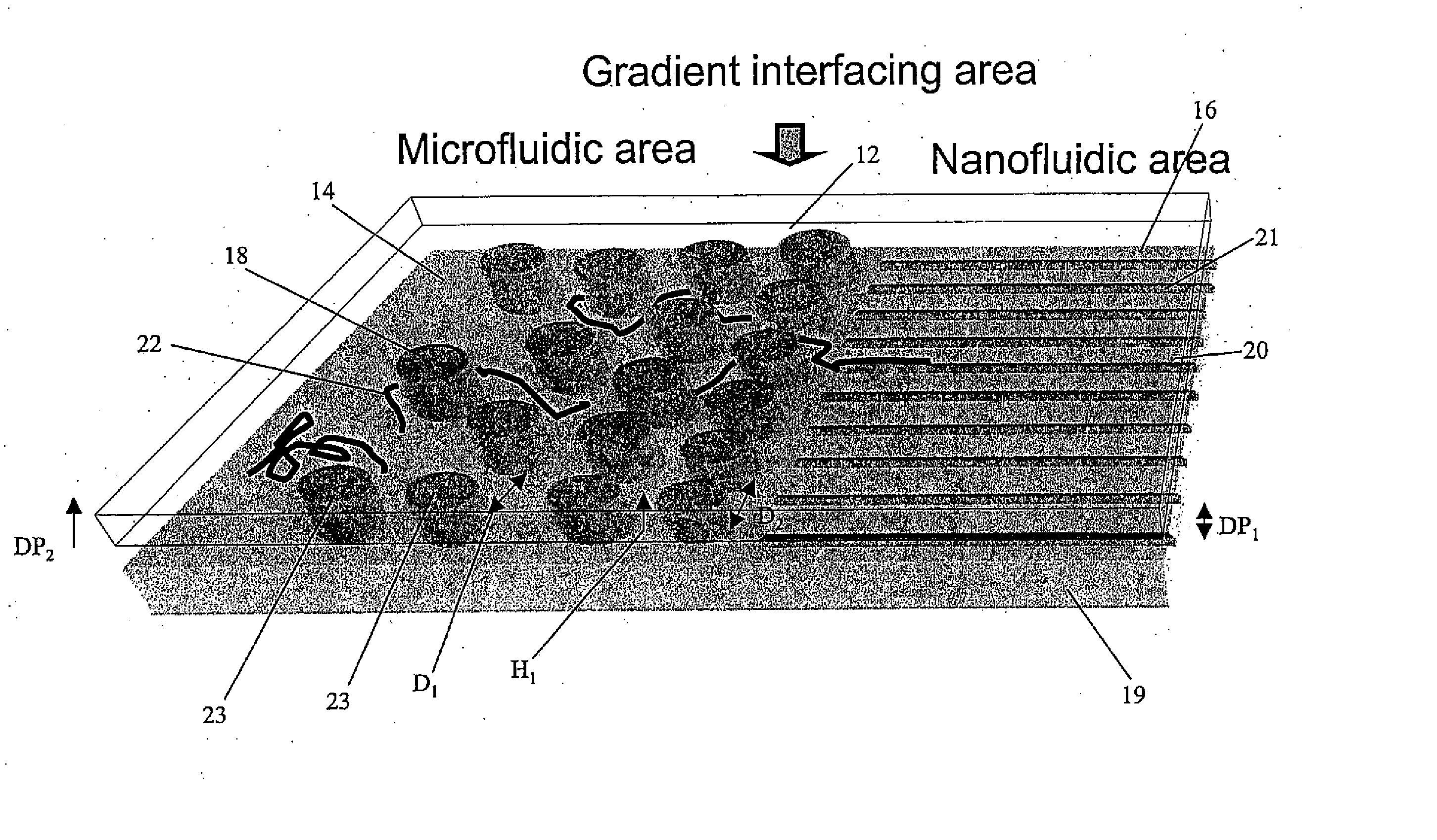
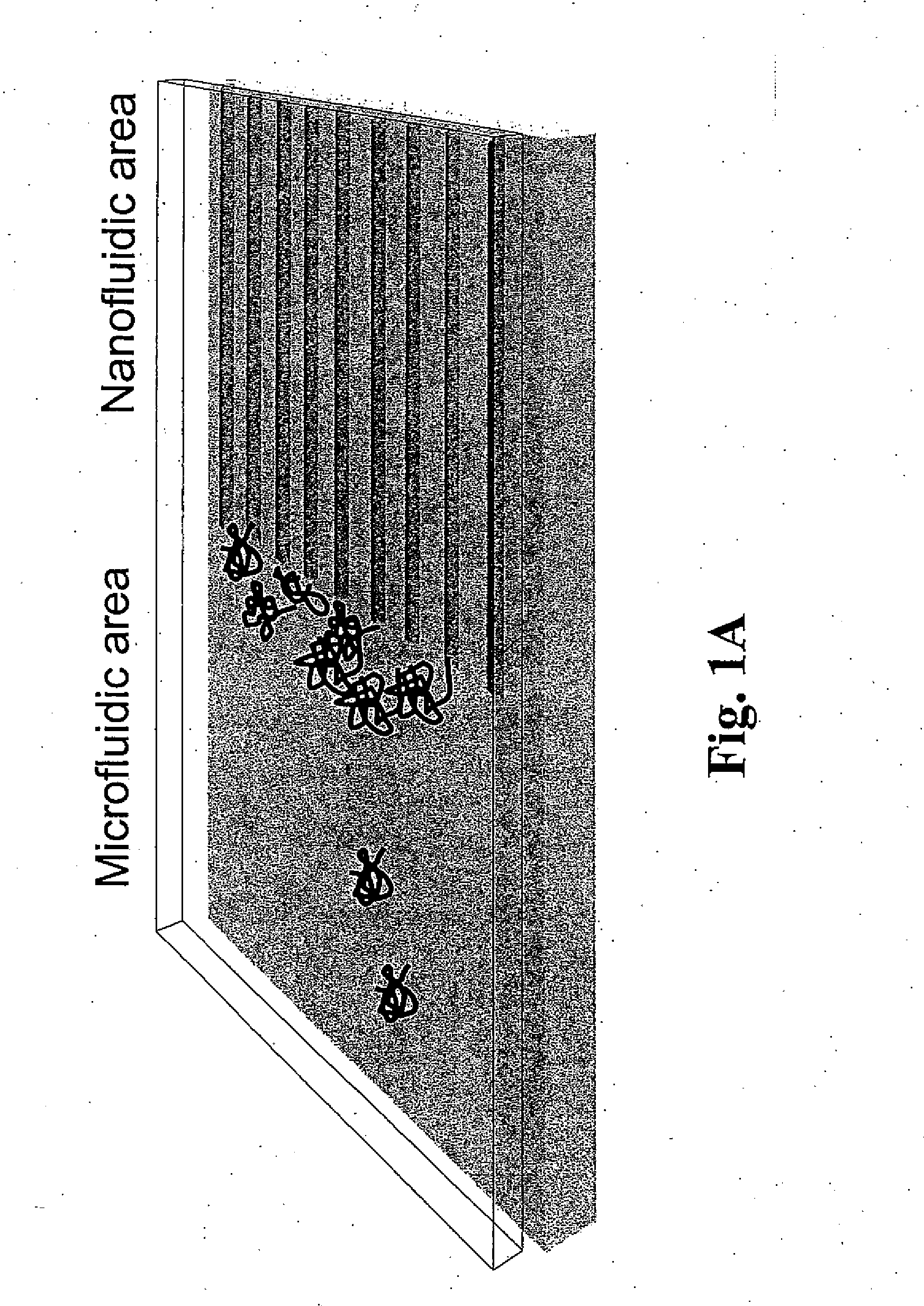
[0079] Large arrays of nanochannels were first fabricated on an entire Si substrate chip using nanoimprinting lithography, described in S. Y. Chou, P. R. Krauss, and P. J. Renstrom, Appl. Phys. Lett. 67 (21), 3114 (1995); Stephen Y. Chou, Peter R. Krauss and Preston J. Renstrom, Science 272, 85 (1996) and U.S. Pat. No. 5,772,905. This chip was spin coated with positive tone photoresist (AZ5214-E) using standard protocol at 4000 rpm for 1 min after HMDS treatment and baked at 110° C. for 2 min. A Karl Suss MA-6 contact aligner and a uniform micron feature size hexagon array photomask were used to pattern the microfluidic area. A blocking mask of a piece of aluminum foil was placed on top of the photomask. The distance between the blocking mask and the photoresist surface was about 3 mm. The chip was exposed at 400 nm UV light in hard contact mode for 35 seconds and developed with a standard procedure (AZ312 MIF: H2O 1:1). The photoresist was used as an etching mask during a subsequen...
PUM
| Property | Measurement | Unit |
|---|---|---|
| Length | aaaaa | aaaaa |
| Length | aaaaa | aaaaa |
| Length | aaaaa | aaaaa |
Abstract
Description
Claims
Application Information
 - R&D
- Intellectual Property
- Life Sciences
- Materials
- Tech Scout
- Unparalleled Data Quality
- Higher Quality Content
- 60% Fewer Hallucinations
Browse by: Latest US Patents, China's latest patents, Technical Efficacy Thesaurus, Application Domain, Technology Topic, Popular Technical Reports.
© 2025 PatSnap. All rights reserved.Legal|Privacy policy|Modern Slavery Act Transparency Statement|Sitemap|About US| Contact US: help@patsnap.com


