ESD protection structure

a protection structure and shielding technology, applied in the direction of amplifier protection circuit arrangement, emergency protection arrangement for limiting excess voltage/current, electrical equipment, etc., can solve the problems of undesirable signal distortion at high hf power levels, irreversible changes in its components or assemblies, etc., to achieve reliable protection effect and improve modulation capability.

Inactive Publication Date: 2006-11-30
ATMEL GERMANY
View PDF7 Cites 18 Cited by
  • Summary
  • Abstract
  • Description
  • Claims
  • Application Information

AI Technical Summary

Benefits of technology

[0010] It is therefore an object of the present invention to provide an ESD protection circuit and a circuit arrangement using the former, which offer a reliable protective effect with improved modulation capability in the HF range without resulting in signal distortion during operation, wherein the proposed ESD protection circuit must also be simple and flexible to use in its circuit design.
[0011] The object is attained by an ESD protection structure of the aforementioned type in that the pn junctions of the two semiconductor diodes possess a common zone of semiconductor material of a first conductivity type, and in that the other zone of each pn junction of the two semiconductor diodes is freely connectable. This achieves, in particular, a significant increase (in terms of amount) in the breakdown voltage, which has a positive effect on the modulation capacity of a subsequent circuit and on the available signal quality. Moreover, due to the reduced surface dimensions as compared to conventional diodes, the special design of the diode structure with common zone that is employed in accordance with the invention contributes to a reduction in parasitic capacitance to the substrate, so that the diode structure is suitable for higher frequencies.
[0013] In this context, according to an embodiment of the invention, the semiconductor diodes can be, for example, Zener diodes. In this way, according to the invention the (negative) breakdown voltage can be displaced to a value Vmin≈−7 V, with the result that no distortion of the signal occurs, even at high HF power.
[0017] A further embodiment of the present invention provides an isolating zone to electrically isolate the other zones of the pn junction from one another and from the semiconductor substrate, in particular by providing a trench filled with an appropriate oxide, a field oxide, or a suitable separating implantation. In order to keep the complexity of construction of the ESD protection structure thus created as small as possible, further provision can be made for the isolating zone to be made thin in comparison with a vertical overall dimension of the ESD protection structure, i.e. in comparison to its depth, thus resulting, in particular, in corresponding size and cost advantages over prior art protective structures having thick epitaxial layers.

Problems solved by technology

If signals of this nature, whose amplitude can be several kV, are fed to an integrated circuit, irreversible changes in its components or assemblies can occur, for example by burn-through of thin layers (thin-film burn-out), filamentation and short-circuiting of layer junctions (junction spiking), charge carrier injection in oxide layers (charge injection or oxide rupture), which under some circumstances leads to destruction of the entire IC.
In this way, the ESD protection can lead to undesirable signal distortions at high HF power levels.
The prior art series connection of multiple forward-biased diodes brings no improvement here, as the parasitic parallel substrate diodes that are present in the integrated design generally employed today will in any case become conducting with the aforementioned terminal voltage.
One side of one of the diodes here is permanently connected to ground or the substrate, resulting in a limited usability of the proposed ESD protection circuit.

Method used


Image

  • ESD protection structure
  • ESD protection structure

Examples


Embodiment Construction

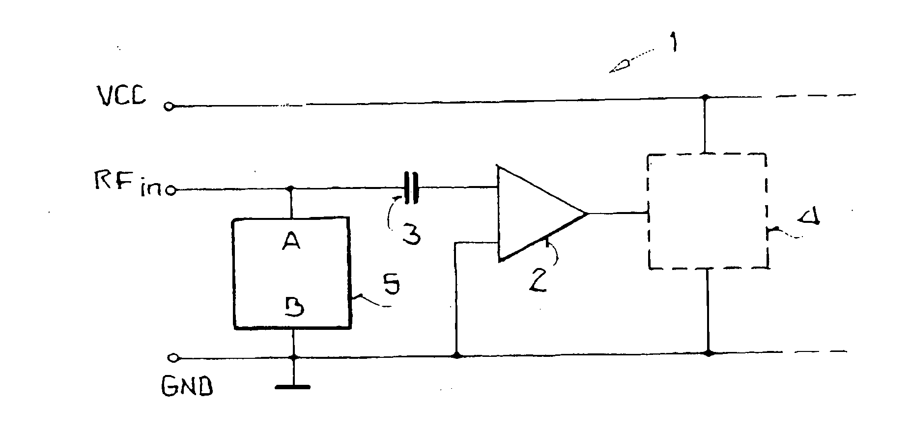
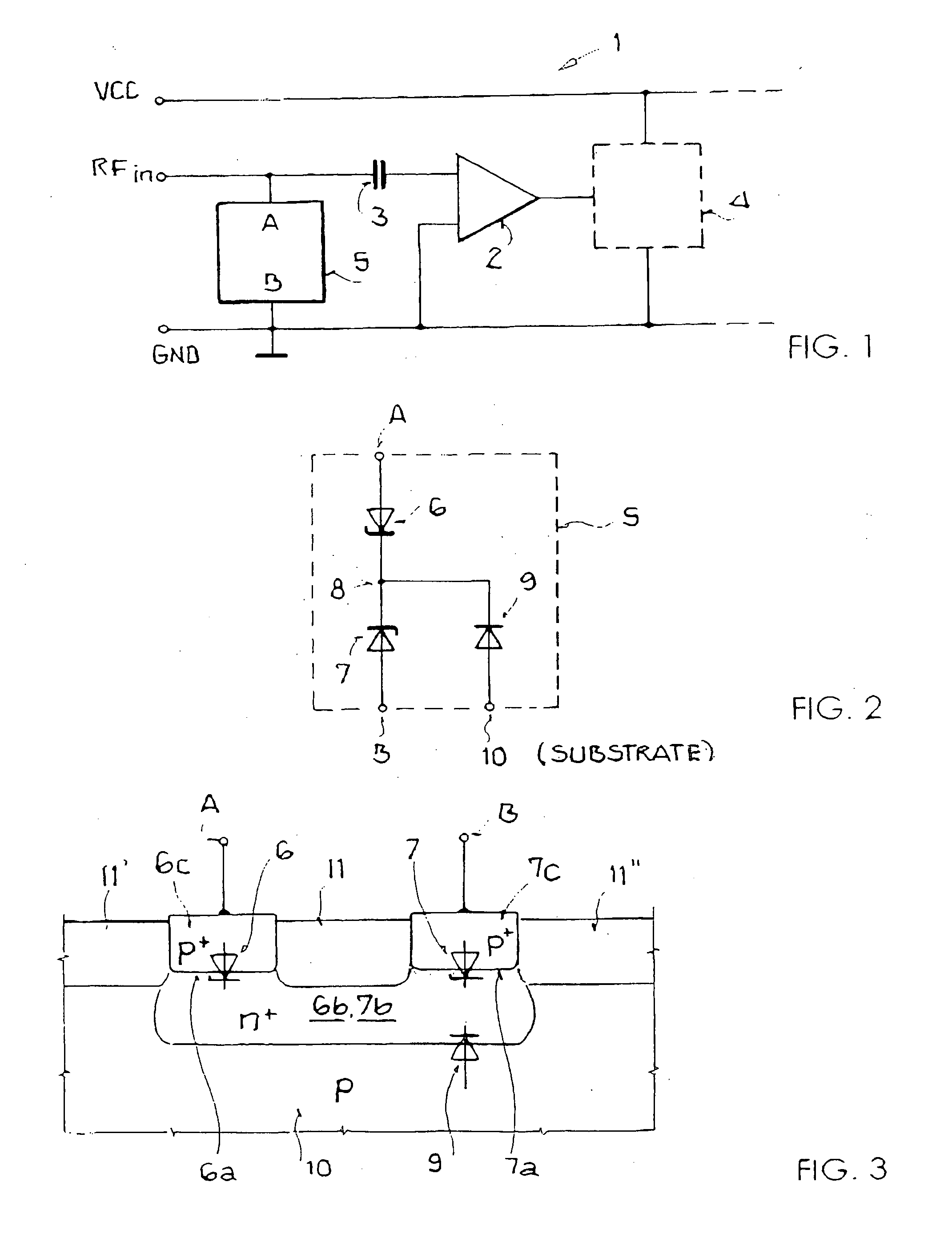
[0026]FIG. 1 shows a block diagram of a circuit arrangement 1 for processing an electrical signal, in particular in the high frequency range (HF range), for example at 868 MHz. The circuit arrangement 1 includes a first input RFin for the signal to be processed, and also a second input GND for a reference voltage, preferably ground. In addition, the circuit arrangement 1 has a processing unit 2 for processing the electrical signal; according to the embodiment depicted, the processing unit can be a bipolar amplifier for RF signals in the HF range. This amplifier has a signal connection to at least the first input RFin, whereby the amplifier shown in FIG. 1 is additionally connected on an input side to a capacitor 3 in the manner of a high pass filter, resulting in what is called an active filter circuit.

[0027] Following the processing unit 2, the circuit arrangement 1 can includes additional circuit components 4, not described here in detail (shown in dashed lines in FIG. 1), which ...


PUM


Abstract

An ESD protection structure for an electronic circuit arrangement, in particular for a HF power amplifier is provided. In the ESD protection structure, at least two semiconductor diodes are connected anti-serial to one another. Further, the pn junctions of the two semiconductor diodes possess a common zone of semiconductor material of a certain conductivity type. Thus, an ESD protection structure is provided that can be used even at relatively high frequencies, which offers a reliable protective effect in the event of overvoltages with improved modulation capability in the HF range without resulting in signal distortion during operation.

Description

[0001] This nonprovisional application claims priority under 35 U.S.C. § 119(a) on German Patent Application Nos. DE 102005025400 and DE 102005057614, which were filed in Germany on May 31, 2005 and Dec. 2, 2005, respectively, and which are herein incorporated by reference. BACKGROUND OF THE INVENTION [0002] 1. Field of the Invention [0003] The present invention relates to an ESD protection structure for an electronic circuit arrangement, in particular for a high frequency (HF) power amplifier, which can be connected between a reference voltage and a signal input of the circuit arrangement, having an electrical valve to limit a possible differential voltage between the signal input and the reference voltage, wherein the valve has at least one arrangement of two semiconductor diodes connected anti-serial to one another. [0004] The invention also relates to a circuit arrangement for processing an electrical signal, in particular in the HF range, for example at 868 MHz in the ISM frequ...

Claims


Application Information

Patent Timeline
Patent Type & Authority Applications(United States)
IPC IPC(8): H02H9/00
CPCH01L27/0255H03F2200/444H03F3/195H03F1/52
Inventor BISCHOF, WERNER
Owner ATMEL GERMANY
Why Eureka
Try Eureka