
Superhard cutters and associated methods

a cutter and super-hard technology, applied in the direction of grinding devices, lapping machines, other chemical processes, etc., can solve the problems of a large number of problems, the surface of silicon wafers may become chipped, and the conventional process is relatively expensive and not always effectiv

Inactive Publication Date: 2006-11-16
SUNG CHIEN MIN
View PDF81 Cites 65 Cited by
  • Summary
  • Abstract
  • Description
  • Claims
  • Application Information

AI Technical Summary

Benefits of technology

[0011] In accordance with another aspect of the invention, a product is provided that can be formed by the process comprising: engaging a surface of a workpiece with a plurality of individual cutting elements of a cutting device, the individual cutting elements being integrally formed from a working side of an integral piece of a polycrystalline superhard material and each cutting element having a peak that is aligned in a common plane; and moving the workpiece and the cutting device relative to one another to thereby remove material from the workpiece with the cutting elements.

Problems solved by technology

While this well-known process has been used successfully for many years, it suffers from a number of problems.
For example, this conventional process is relatively expensive and is not always effective, as the silicon wafers may not be uniform in thickness, nor may they be sufficiently smooth, after completion of the process.
In addition to becoming overly “wavy” when etched by a solvent, the surface of the silicon wafers may become chipped by individual abrasive grits used in the process.
Moreover, if the removal rate is to be accelerated to achieve a higher productivity, the grit size used on the polishing pad must be increased, resulting in a corresponding increase in the risk of scratching or gouging expensive wafers.
Furthermore, because surface chipping can be discontinuous, the process throughput can be very low.
Consequently, the wafer surface preparation of current state-of-the-art processes is generally expensive and slow.
While diamond grid pad conditioners have been effectively used in dressing CMP pads for polishing previous designs of integrated circuitry, they have not been found suitable for making cutting-edge devices with nodes smaller than 65 nm.
This is because, with the decreasing size of the copper wires, non-uniform thickness due to rough- or over-polishing will change the electrical conductivity dramatically.
However, the more delicate the polishing process becomes, the higher the risk of scratching the surface of the wafer becomes.
Otherwise, the protrusion of a few “killer asperities” can ruin the polished wafer.

Method used


Image

  • Superhard cutters and associated methods
  • Superhard cutters and associated methods
  • Superhard cutters and associated methods

Examples


example 1

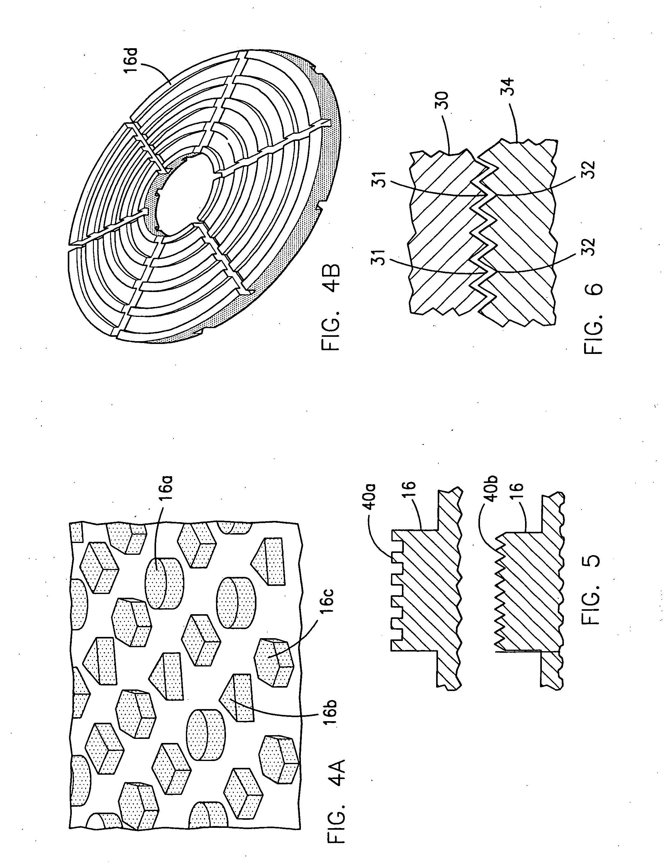
[0079] A boron doped diamond film (“BDD”) having a resistivity of about 0.001 ohm-cm and a thickness of about 500 μm has a “zigzag” pattern formed on one edge via a wire EDM process. The resulting blade is mounted on an EDM machine as a cathode. The anode is a flat PCD about 100 mm in diameter and about 2 mm in thickness. The diamond table used is about 500 μm in thickness. An electrically conducting fluid is used to carry the electricity between the two electrodes. During the EDM process, the PCD is gradually traversed across the stationary BDD blade. This process is repeated while the BDD is gradually descending into the PCD compact. The portion of the PCD that is brought in close proximity to the edge of the BDD is selectively eroded away by electrical discharging, electrolysis, and dissolution.

[0080] In this manner, a corresponding “zigzag” pattern of ridges is gradually formed on the flat PCD top. When the grooves reach a predetermined height (e.g., 80 μm), the serrated ridges...

example 2

[0082] The above example was repeated with the reverse polarity: e.g., the BDD was positively biased. In this case, the EDM process was still viable except that the wear rate of the BDD was more than doubled. However, the surface finish of the ADD improved due to a slower erosion rate on the surface.

example 3

[0083] The process of Example 1 was repeated except that the cathode was replaced by a PCD blank of 1.6 mm in thickness (PCD table 0.5 mm thick, cemented tungsten carbide 1.5 mm thick). The PCD used had a 25 μm diamond grain size, it contained 10 wt % of cobalt and had an electrical resistivity of 0.001 ohm-cm.


PUM


Abstract

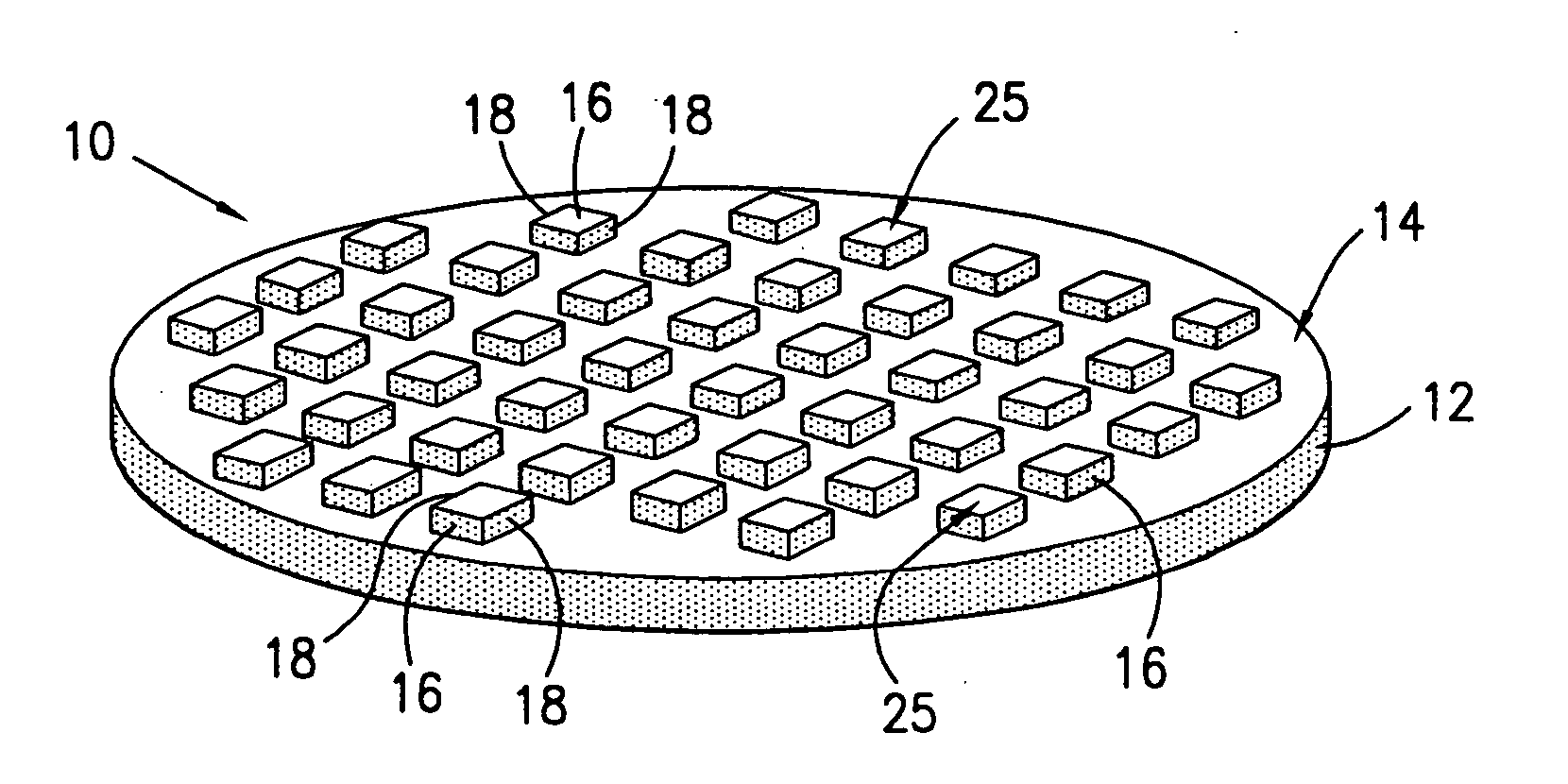
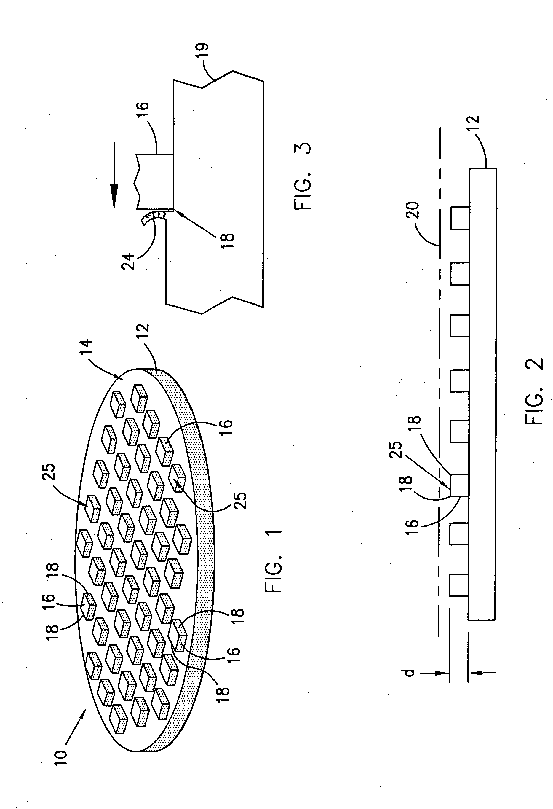
A cutting device comprises a base having a working side that is oriented to face a workpiece from which material is to be removed. A plurality of individual cutting elements are arranged on the working side of the base, with each cutting element having a peak that comprises at least one cutting edge that is formed from a polycrystalline superhard material. The peaks of the cutting elements are aligned in a common plane.

Description

PRIORITY DATA [0001] This application claims priority to copending U.S. Provisional Patent Application No. 60 / 681,798, filed May 16, 2005, which is hereby incorporated herein by reference in its entirety.FIELD OF THE INVENTION [0002] The present invention relates generally to cutting devices used to plane workpieces formed of various materials. Accordingly, the present invention involves the fields of chemistry, physics, and materials science. BACKGROUND OF THE INVENTION [0003] It is estimated that the semiconductor industry currently spends more than one billion U.S. Dollars each year manufacturing silicon wafers that exhibit very flat and smooth surfaces. Typically, chemical mechanical polishing (“CMP”) is used in the manufacturing process of semiconductor devices to obtain smooth and even surfaced wafers. In a conventional process, a wafer to be polished is generally held by a carrier positioned on a polishing pad attached above a rotating platen. As slurry is applied to the pad ...

Claims


Application Information

Patent Timeline
IPC IPC(8): B24D3/00B24D18/00B24D11/00
CPCB24D7/06B24B7/228B24B37/24B24D11/00B24B37/00H01L21/304
Inventor SUNG, CHIEN-MIN
Owner SUNG CHIEN MIN
Learn More