Method of fabricating memory device utilizing carbon nanotubes

a memory device and carbon nanotube technology, applied in the field of memory devices, can solve the problems of inability to adjust the current flow, inability to manufacture memory devices, and inability to meet the needs of users, etc., and achieve the effects of high electrical conductivity, increased resistance and malfunction, and increased resistan

Inactive Publication Date: 2006-11-09
SAMSUNG ELECTRONICS CO LTD
View PDF7 Cites 15 Cited by
  • Summary
  • Abstract
  • Description
  • Claims
  • Application Information

AI Technical Summary

Benefits of technology

[0012] The present invention provides a fast, highly-integrated memory device capable of preventing an increase in resistance caused by miniaturization of the memory device, and capable of providing low thermal loss, low power consumption, stable electrical characteristics, and a low charge leakage.
[0013] According to a feature of an embodiment of the present invention, there is provided a carbon nanotube memory device including a substrate, a source electrode and a drain electrode arranged with a predetermined interval between them on the substrate and subjected to a voltage, a carbon nanotube connecting the source electrode to the drain electrode and serving as a channel for charges, a memory cell, located over the carbon nanotube, that stores charges from the carbon nanotube, and a gate electrode, formed in contact with the upper surface of the memory cell, for controlling the amount of charge flowing from the carbon nanotube into the memory cell.
[0022] According to another feature of an embodiment of the present invention, there is provided a method of fabricating a carbon nanotube memory device including: (a) growing a carbon nanotube on a substrate and forming a source electrode and a drain electrode in contact with the carbon nanotube such that the carbon nanotube between the source electrode and the drain electrode serves as a charge moving channel; (b) forming a memory cell in contact with the carbon nanotube by sequentially depositing a first insulating film, a charge storage film, and a second insulating film on the carbon nanotube, the source electrode, and the drain electrode, and patterning the resultant structure using a photolithographic method; and (c) forming a gate electrode which controls the amount of charge flowing from the carbon nanotube into the charge storage film by depositing a metal layer on the second insulating film and patterning the resultant structure using a photolithographic method.
[0034] In the present invention, because a carbon nanotube is used as a charge moving channel, a doping process for a semiconductor memory device is not required. Furthermore, because a carbon nanotube having a high electrical conductivity and a high thermal conductivity is used, an increase in resistance and malfunction due to the high-integration of a memory device are prevented. Also, because the memory device according to the present invention includes the charge storage film to store charge, or a porous film having nanodots, the memory device functions as a highly efficient, highly-integrated memory device.

Problems solved by technology

However, manufacturing highly integrated memory devices requires reducing the physical size of MOSFETs, which in turn requires reducing the physical sizes of gate, source, and drain electrodes, which leads to a variety of problems.
When reducing the size of a MOSFET, a distance between a source and a drain may be decreased, generating a phenomenon known as “punch through,” in which the source and a depletion layer of the drain come into contact, making it impossible to adjust the current flow.
Increased electrical resistance, punch through, and decreased channel width in MOSFETs result in heat loss, increased power consumption, electrical characteristic variations, charge leakage, etc., ultimately causing unacceptable memory device function.
Therefore, reducing the size of MOSFETs to create highly integrated semiconductor memory devices is limited by the inherent physical characteristics of MOSFETs.
As a result, general memory devices based on MOSFETs are not suitable for use as future high-density memory devices, and an alternative is needed.

Method used


Image

  • Method of fabricating memory device utilizing carbon nanotubes
  • Method of fabricating memory device utilizing carbon nanotubes
  • Method of fabricating memory device utilizing carbon nanotubes

Examples


Embodiment Construction

[0054] This application relies for priority upon Korean Patent Application No. 2002-7709, filed Feb. 9, 2002, and Korean Patent Application No. 2002-71398, filed Nov. 16, 2002, the contents of which are incorporated herein by reference in their entirety.

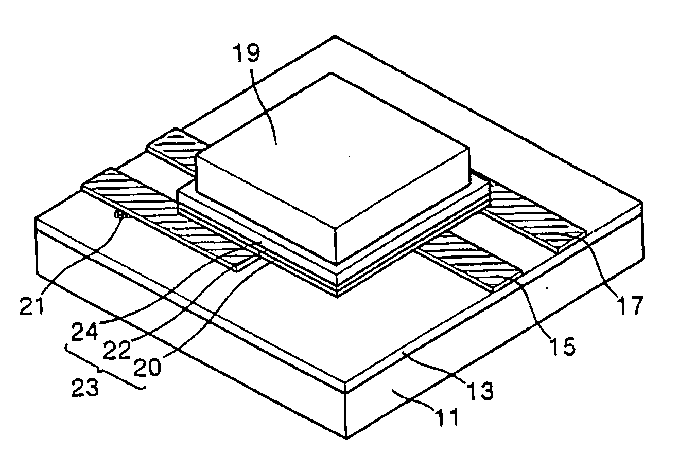
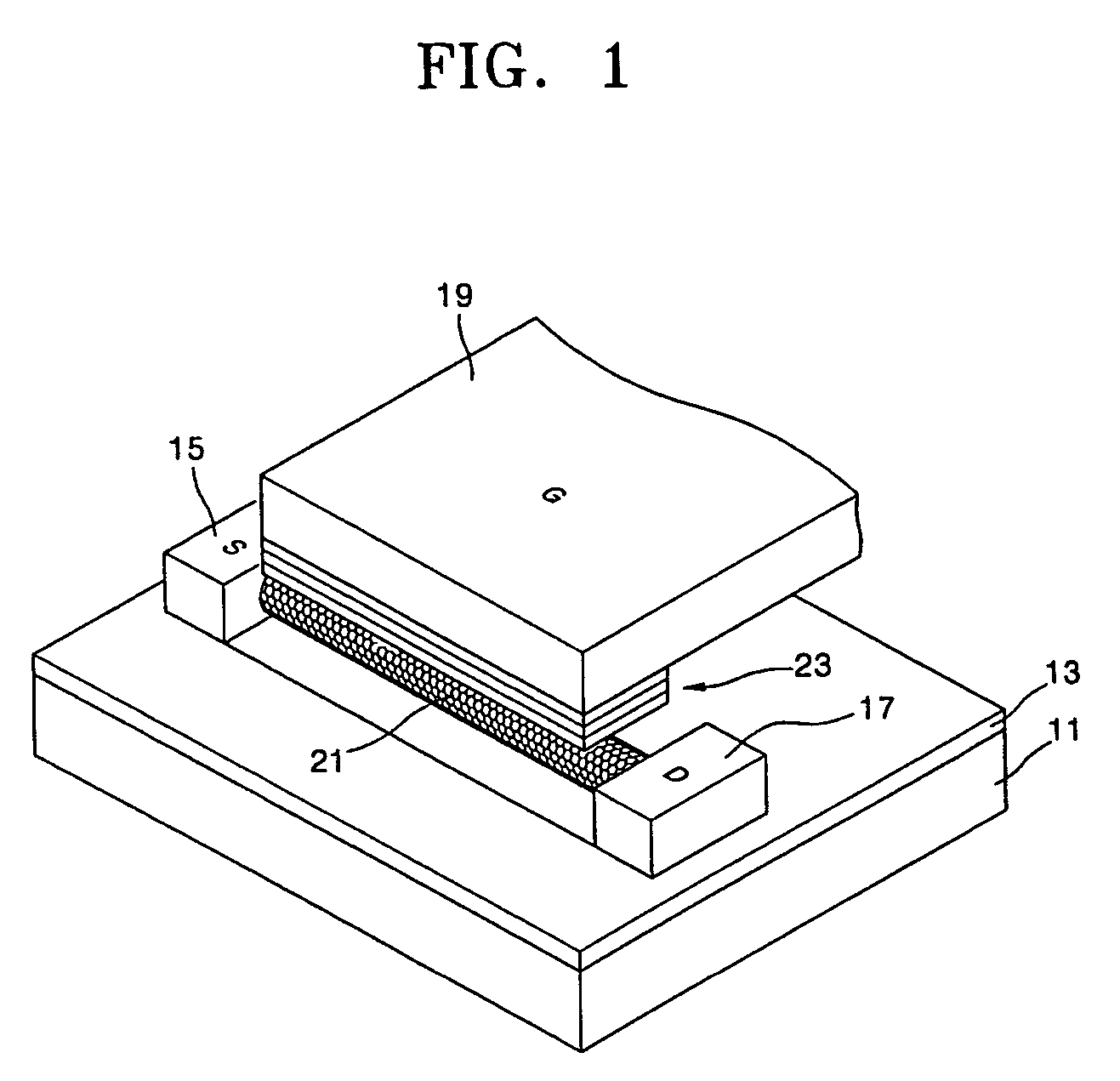
[0055] Referring to FIG. 1, a memory device according to an embodiment of the present invention includes a substrate 11, an insulating layer 13 deposited on the substrate 11, a source electrode 15 and a drain electrode 17 which are made of metal and separated by a predetermined distance from each other on the insulating layer 13, a carbon nanotube 21 which connects the source electrode 15 to the drain electrode 17 and serves as an electron moving channel, a memory cell 23 which contacts the carbon nanotube 21 and stores charges of electrons (or holes), and a gate electrode 19 which contacts the memory cell 23 and controls the movement of the electrons.

[0056] In FIG. 1, the source and drain electrodes 15 and 17 are installed on the ...


PUM

PropertyMeasurementUnit
thicknessaaaaaaaaaa
sizeaaaaaaaaaa
drain currentaaaaaaaaaa

Abstract

A fast, reliable, highly integrated memory device formed of a carbon nanotube memory device and a method for forming the same, in which the carbon nanotube memory device includes a substrate, a source electrode, a drain electrode, a carbon nanotube having high electrical and thermal conductivity, a memory cell having excellent charge storage capability, and a gate electrode. The source electrode and drain electrode are arranged with a predetermined interval between them on the substrate and are subjected to a voltage. The carbon nanotube connects the source electrode to the drain electrode and serves as a channel for charge movement. The memory cell is located over the carbon nanotube and stores charges from the carbon nanotube. The gate electrode is formed in contact with the upper surface of the memory cell and controls the amount of charge flowing from the carbon nanotube into the memory cell.

Description

CROSS REFERENCE TO RELATED APPLICATION(S) [0001] This is a divisional application based on pending application Ser. No. 10 / 361,024, filed Feb. 10, 2003, the entire contents of which is hereby incorporated by reference.BACKGROUND OF THE INVENTION [0002] 1. Field of the Invention [0003] The present invention relates to a memory device and a method of fabricating the same. More particularly, the present invention relates to a memory device including a carbon nanotube that serves as a charge moving channel and a method of fabricating the memory device. [0004] 2. Description of the Related Art [0005] Semiconductor memory devices fundamentally include a capacitor that preserves stored charges and a transistor that serves as a switch for securing a path of current necessary to write data to or read data from the capacitor. [0006] To allow a high current to flow in a transistor, the transistor must have a high transconductance (gm). Hence, metal oxide field effect transistors (MOSFETs) havi...

Claims


Application Information

Patent Timeline
Patent Type & Authority Applications(United States)
IPC IPC(8): H01L21/31B82B1/00B82B3/00G11C13/02H01L21/8247H01L27/115H01L29/06H01L29/788H01L29/792
CPCB82Y10/00Y10S977/943G11C2213/17G11C13/025
Inventor CHOI, WON-BONGYOO, IN-KYEONGCHU, JAE-UK
Owner SAMSUNG ELECTRONICS CO LTD
Why Eureka
Try Eureka