Light deflector, light deflection array, optical system, image forming device, and projection type image display apparatus

Inactive Publication Date: 2006-10-26
RICOH KK
View PDF12 Cites 20 Cited by
  • Summary
  • Abstract
  • Description
  • Claims
  • Application Information

AI Technical Summary

Benefits of technology

[0040] The above object of the present invention is to provide a light deflector, light deflection array, optical system, image forming device, and projection type image display apparatus, wherein an optional part (contact part or fulcrum part) on the substrate or a corresponding contact part of a plate-shaped member where the plate-shaped member (mirror) comes in contact when being tilted and displaced is made of a heat resistant (high melting point) film and with little mechanical deformation (namely hardness) so that the fixing by the acting force is prevented and the low voltage driving of the light deflector is implemented.
[0041] The above object of the present invention is also to provide a light deflector, light deflection array, optical system, image forming device, and projection type image display apparatus, wherein an optional part of a stopper facing the plate-shaped member is made of a rigid (hard) layer so that the fixing of the plate-shaped member to the stopper is prevented and the low voltage driving of the light deflector is implemented.
[0183] According to the above-mentioned aspect of the invention, it is possible to provide a light deflector, light deflection array, optical system, image forming device, and projection type image display apparatus, wherein an optional part (contact part or fulcrum part) on the substrate or a corresponding contact part of a plate-shaped member where the plate-shaped member (mirror) comes in contact when being tilted and displaced is made of a heat resistant (high melting point) film and with little mechanical deformation (namely hardness) so that the fixing by the acting force is prevented and the low voltage driving of the light deflector is implemented.
[0184] It is also possible to provide a light deflector, light deflection array, optical system, image forming device, and projection type image display apparatus, wherein an optional part of a stopper facing the plate-shaped member is made of a rigid (hard) layer so that the fixing of the plate-shaped member to the stopper is prevented and the low voltage driving of the light deflector is implemented.

Problems solved by technology

In order to tilt and displace the plate-shaped member beyond the fixing force, it is necessary to increase voltage applied to plural electrodes and this causes obstacles to a low voltage driving the light deflector.
Thus, there is a problem in not only the light deflector giving the electric potential to the plate-shaped member via the fulcrum member but also the light deflector displacing the electrically floating plate-shaped member.
Increase of the reset voltage may make low voltage driving of the light deflector difficult and increase the consumption of electric power of products using the light deflector such as the optical system, image forming device, and projection type image display apparatus.
The contact at the film having such a surface roughness may not be influenced by the fixing due to the force between the molecules because the distance is too long.
The light deflection at the driving voltage of several volts is difficult and therefore application of the driving voltage equal to or greater than 10 V is necessary for beginning the light deflection operation by overcoming fixing.

Method used


Image

  • Light deflector, light deflection array, optical system, image forming device, and projection type image display apparatus
  • Light deflector, light deflection array, optical system, image forming device, and projection type image display apparatus
  • Light deflector, light deflection array, optical system, image forming device, and projection type image display apparatus

Examples


first example

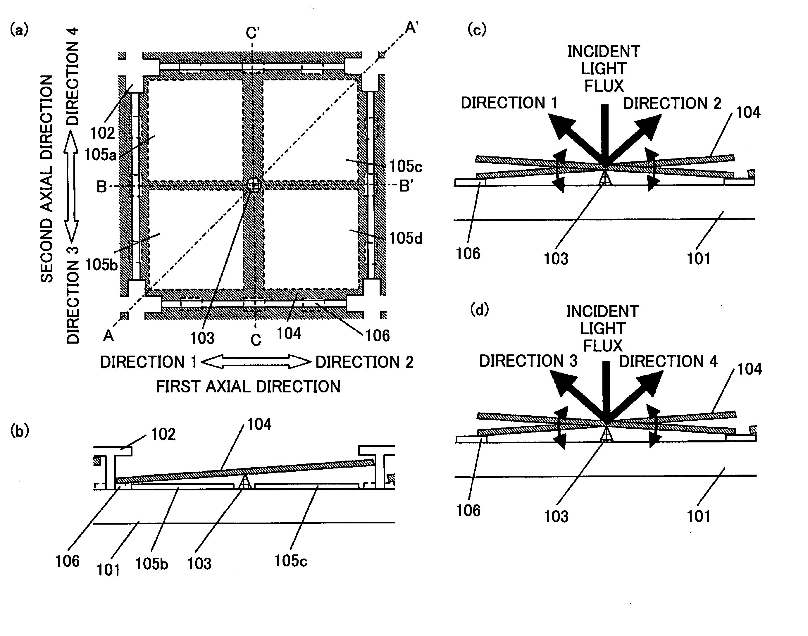
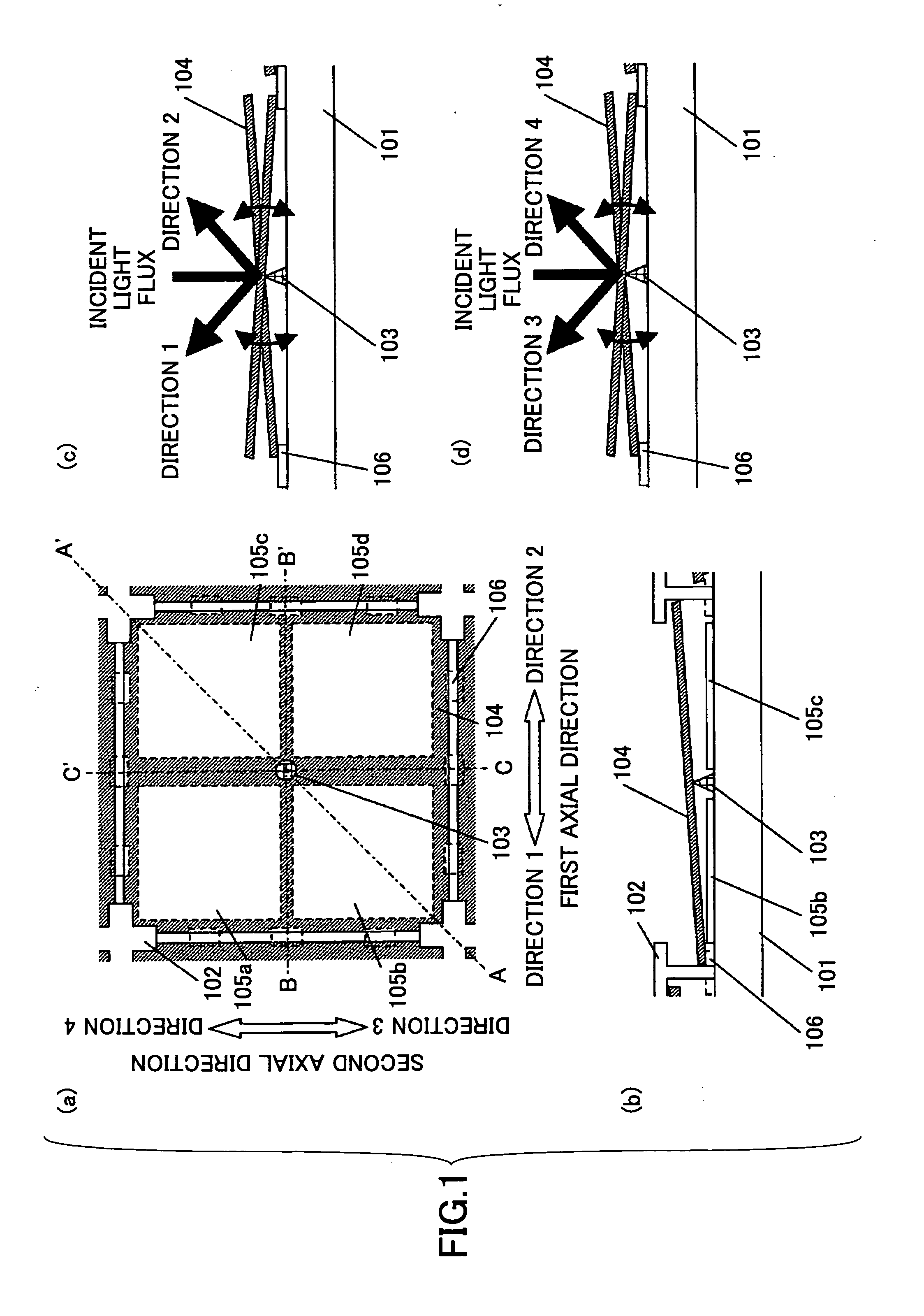
[0213]FIG. 5 is an A-A′ cross-sectional view (see FIG. 1(a)) of a light deflector of a first example of the present invention. In the first example, a lower layer 104a of the plate-shaped member 104, in addition to the fulcrum member 103 and the contact part 106, is formed by a layer (shown in gray color) whose main ingredient is a high melting point metal element. In addition, an aluminum group metal film having a high reflection ratio is formed on an upper layer of the plate-shaped member 104.

[0214] The lower layer 104a whose main ingredient is the high melting point metal element is defined as including 50 wt % or more of the high melting point metal element. More specifically, the lower layer 104a may be a single layer film, an alloy film, a nitride firm, or oxide film of titanium, zirconium, tantalum, chrome, molybdenum, or tungsten.

[0215] In the first example, the tungsten single layer film is used. The lower layer 104a has a high heating resistance, high Young's modulus and...

second example

[0217]FIG. 6 is an A-A′ cross-sectional view of a light deflector of a second example of the present invention. In the second example, an upper layer 103a of a fulcrum member 103, an upper layer 106a of a contact part 106, and a lower layer 104a of a plate-shaped member 104 are formed by titanium nitride film. An aluminum group metal film having a high reflection ratio is formed on an upper layer of the plate-shaped member 104. The fulcrum member 103 and the contact part 106 are formed, if necessary, by an insulation film such as a silicon oxide film or a conductive film such as the aluminum group metal film.

[0218] In the second example, while the titanium nitride film is formed on the upper layer 103a of the fulcrum member 103 and the upper layer 106a of the contact part 106, the present invention is not limited to this.

[0219] While the titanium nitride film of the second example is a nitride film, the titanium nitride film has a conductivity of approximately 2 E-4 Ωcm, a melting...

third example

[0221]FIG. 7 shows a light deflection array where plural light deflectors of the first example are arranged in a two dimensional array. More specifically, FIG. 7(a) is an upper surface view of the light deflection array of the third example and FIG. 7(b) is an A-A′ cross-sectional view of FIG. 7(a).

[0222] In the third example, the light deflectors of the present invention are arranged in m lines×n rows. The light deflector performs the light deflection operation as corresponding to a supplied driving signal. Since the low voltage driving of the light deflector at the time of the light deflection can be made, the supplied driving signal may have the low voltage.

[0223] The driving signal is stored in a semiconductor memory circuit formed right below the light deflector so as to let all of the light deflectors perform light deflection operations. For example, as discussed in Japanese Laid-Open Patent Application Publication No. 2004-320821, data designating a tilt direction of the pl...


PUM


Abstract

A light deflector includes a substrate; a plurality of control members provided at edge parts of the substrate, the control members having upper parts where stoppers are situated; a fulcrum member provided on an upper surface of the substrate, the fulcrum member having a top part; a plate-shaped member movably provided in a space formed by the substrate, the fulcrum member and the stopper, the plate-shaped member having a light reflection area, no fixed end, and a conductive layer; and a plurality of electrodes provided on the substrate, the electrodes facing the conductive layer of the plate-shaped member.

Description

BACKGROUND OF THE-INVENTION [0001] 1. Field of the Invention [0002] The present invention generally relates to light deflectors, light deflection arrays, optical systems, image forming devices, and projection type image display apparatuses, whereby the direction of outgoing light compared to incident light is changed. For example, the present invention can be used for image forming devices such as electro-photographic type printers or copiers, or projection type image display apparatuses such as projectors or digital theater systems. [0003] 2. Description of the Related Art [0004] A light deflection method, light deflector, manufacturing method of the light deflector, and a product where the light deflector is applied, previously invented by inventors of the present invention, are disclosed in Japanese Laid-Open Patent Application Publication No. 2004-78136. [0005] More specifically, a light deflector whereby light deflection in a single axial direction or two axial directions is ma...

Claims


Application Information

Patent Timeline
IPC IPC(8): F21V7/00
CPCG02B26/0841G03B21/14H04N9/3105H04N5/7441G03B21/008
Inventor NANJYO, TAKESHIKATOH, SEIICHIOHTAKA, KOICHI
Owner RICOH KK
Why Eureka
Try Eureka