
Method for fabricating a nonvolatile memory element and a nonvolatile memory element

a nonvolatile memory and memory element technology, applied in the direction of electrical devices, semiconductor devices, material nanotechnology, etc., can solve the problems of scaling limits, compatibility of process, adhesion or chemical binding of organic molecule on substrate, etc., to achieve precise patterning, reduce power consumption, and reduce the effect of memory spa

Inactive Publication Date: 2006-10-19
POLARIS INNOVATIONS
View PDF1 Cites 29 Cited by
  • Summary
  • Abstract
  • Description
  • Claims
  • Application Information

AI Technical Summary

Benefits of technology

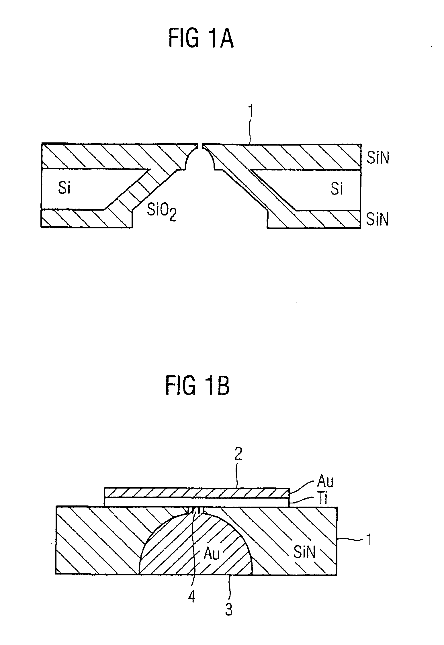
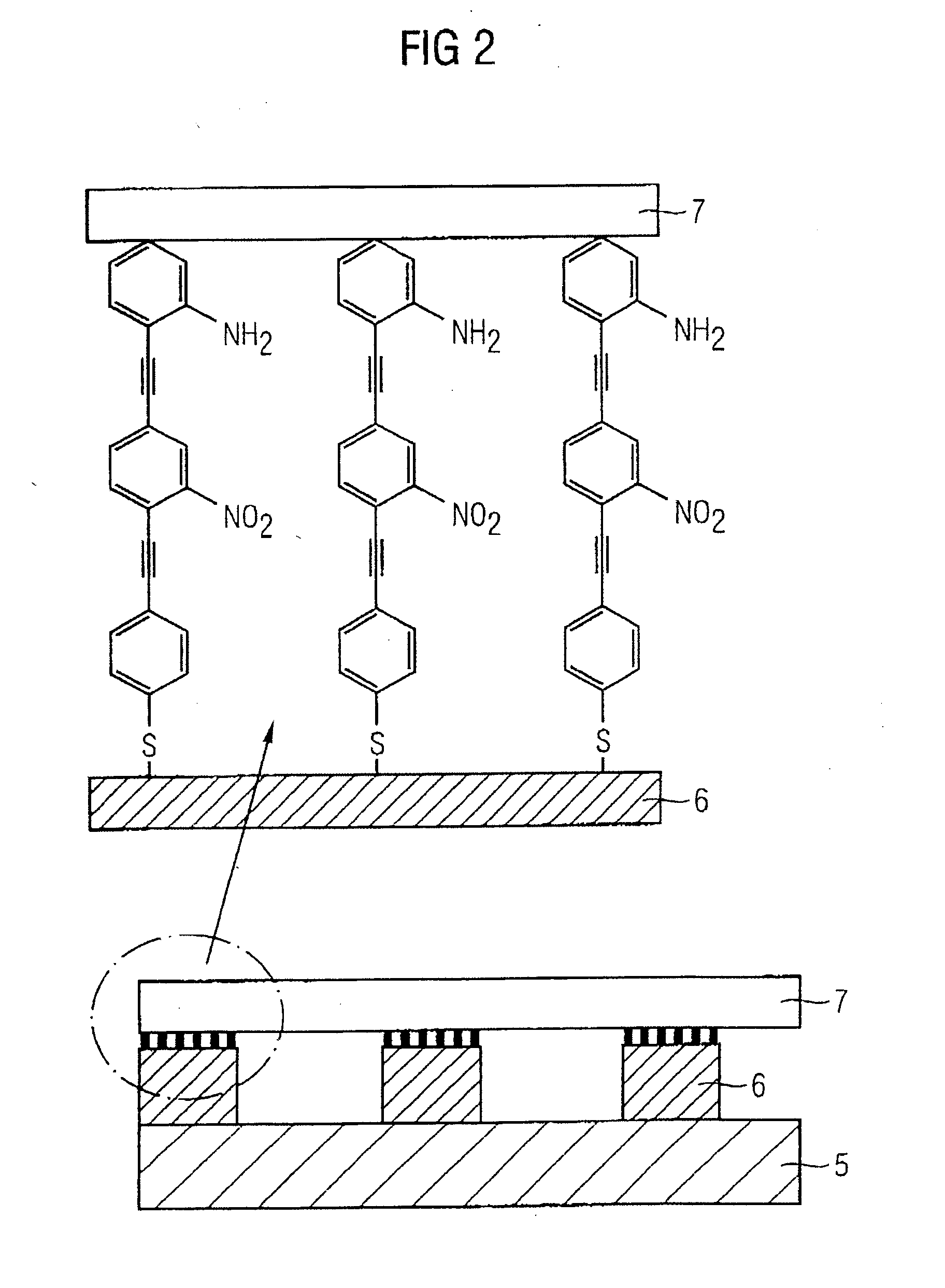
[0021] The organic memory molecules grown on the remaining free area, the effective contact area, can be patterned by means of electron beam lithography without using structure masks in strips having a width of e.g. 20 nm. The strip-type regions with organic molecules grown thereon may have a width of 15 nm to 50 nm. By means of the electrode beam, which can be focused very finely and thus permits precise patterning, the organic memory molecules are removed in the region struck by the beam, e.g. by vaporization or melting and chemical conversion. The underlying layer may be converted e.g. from silicon into silicon oxide. Consequently, it is possible to fabricate a nonvolatile, molecular organic memory element which requires a considerably smaller memory space, manages with a lower power demand and can be implemented with a lower outlay.

Problems solved by technology

The technology for the storage of charges will encounter scaling limits in the foreseeable future.
One problem in the deposition of self-assembled molecular monolayers is the adhesion or chemical binding of the organic molecule on the substrate.
A further problem is the compatibility of the process for fabricating the organic molecular memory element with the existing CMOS technology.
It has not been possible hitherto to satisfactorily realize either the coupling of the organic memory molecule to the substrate or integration of the organic memory molecule into a configuration that is compatible in conventional silicon technology in the dimension range of a few nanometers.
Dense packing of resistive memory cells has not been possible hitherto using this technology.
The integration of gold layers and the chemical mechanical polishing of this material are not possible without problems in the existing CMOS technology.
In addition to the higher costs that occur as a result, the advantage of the small molecular dimensions and the high packing density possible can only be utilized to an unsatisfactory extent in the memory cell configuration realized to date.
The high outlay and the low reproducibility in the application of titanium- or palladium-coated carbon nanotubes as top contacts on the organic memory molecules also constitute a problem.

Method used


Image

  • Method for fabricating a nonvolatile memory element and a nonvolatile memory element
  • Method for fabricating a nonvolatile memory element and a nonvolatile memory element
  • Method for fabricating a nonvolatile memory element and a nonvolatile memory element

Examples


example

[0047] A silicon electrode structure is fabricated on the basis of SOI technology. For this purpose, an oxidized silicon wafer is pressed together with an elemental silicon wafer at high pressure and high temperature and the silicon wafer side is subsequently thinned by means of chemical mechanical polishing (CMP). The silicon tracks are etched by means of currently used silicon etching techniques, such as, e.g. dry etching by means of reactive plasma etching on the basis of HBr and O2 or SF5. A copolymer comprising polynorbornene and poly(norbornene dicarboxylic acid) is subsequently prepared. After the copolymer has been dried it is dissolved again and the stoichiometric amount of SiCl4 dissolved in THF is then added. This solution is applied to the silicon substrate. In this case, the layer grows in a hexagonally ordered manner in a self-assembled process. The silicon salt is converted into silicon oxide by ammonium hydroxide. The copolymer is subsequently removed by plasma ashin...


PUM


Abstract

In a method for fabricating a nonvolatile memory element a substrate is provided, a nanomask structure is fabricated on the substrate and a self-assembled monolayer of an organic memory molecule is grown on the substrate on a region not covered by the nanomask structure. A surface of the substrate is patterned by means of an electrode beam in order to form regions with organic memory molecules and regions without organic memory molecules and a top contact is applied to the monolayer formed from the organic memory molecules and the nanomask.

Description

BACKGROUND OF THE INVENTION [0001] 1. Field of the Invention [0002] The present invention relates to a method for fabricating a nonvolatile memory element and a nonvolatile memory element. [0003] 2. Description of the Related Art [0004] The memory concepts (floating gate memories such as flash and DRAM) used to date are based on the storage of charges in inorganic, silicon-based materials. The technology for the storage of charges will encounter scaling limits in the foreseeable future. Therefore, alternative methods for storing information are increasingly being sought. In this case, the principle of resistive switching between two stable resistance states in organic molecules has proved to be promising. [0005] Conjugated oligophenyleneethynylenes are used in this case as molecular wires in components (with nonlinear 1(V) curves for dynamic random access memories (DRAM)). Such organic molecules, such as e.g. amino4-ethynylphenylbenzenethiol, are grown in a self-assembled monolayer ...

Claims


Application Information

Patent Timeline
IPC IPC(8): H01L51/40
CPCB82Y10/00H01L51/0595B82Y30/00H10K10/701
Inventor UFERT, KLAUS-DIETER
Owner POLARIS INNOVATIONS
Learn More