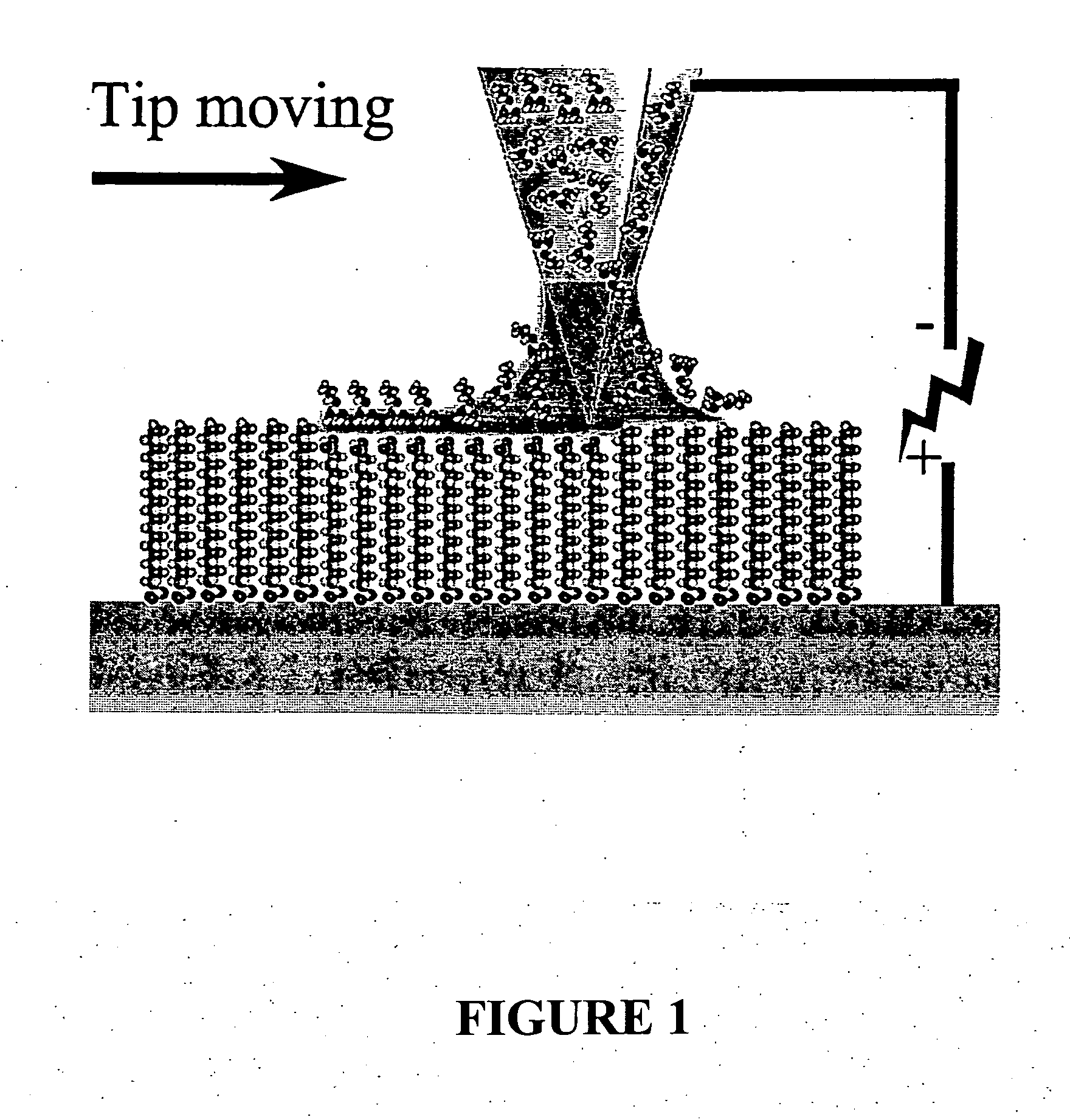
Electropen lithography
a technology of electro-optical probes and lithography, which is applied in the direction of synthetic resin layered products, coatings, transportation and packaging, etc., can solve the problems of nanografting techniques, methods with serious limitations and significant challenges in producing nanoscale patterns
- Summary
- Abstract
- Description
- Claims
- Application Information
AI Technical Summary
Benefits of technology
Problems solved by technology
Method used
Image

Examples
example 1
Preparation of a Substrate
[0233] An octadecyltrichlorosilane (OTS) film was prepared as follows. A silicon wafer was treated with piranha solution for 10 minutes. After drying the wafer under nitrogen, the wafer was soaked for approximately 24 hours in 5 mM OTS bicyclohexyl solution at 20° C. The wafer was then rinsed in chloroform for 30 seconds.
example 2
Patterns Written on OTS Surface Using MPTMS Patterning Molecules
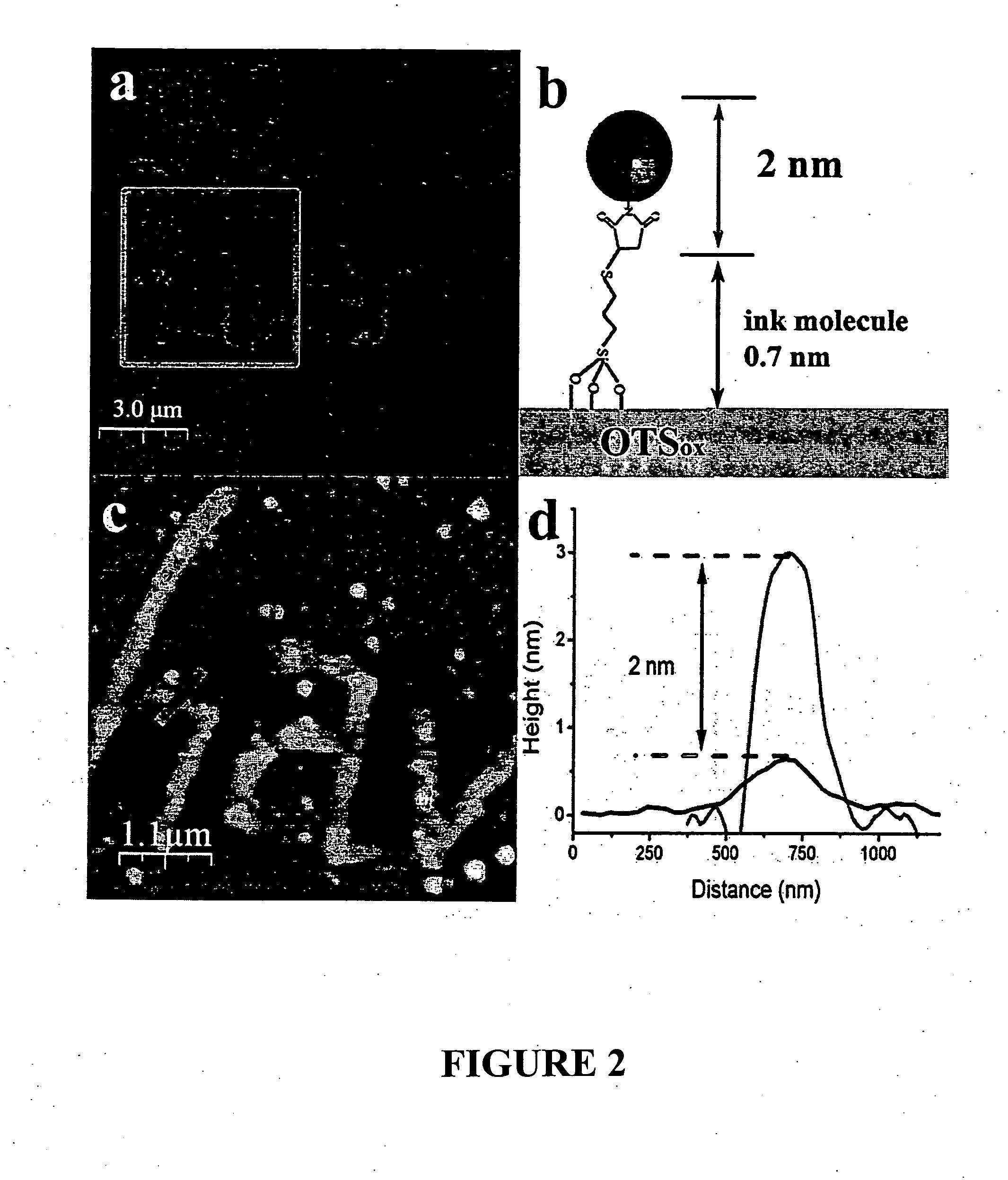
[0234] Shown in FIG. 2 is a pattern of mercaptopropyltrimethoxysilane (MPTMS) patterning molecules written on an OTS surface as prepared above using 9V and 5 μm / s speed (See FIG. 2a). The height of the pattern was measured to be 6.9±1.3 Å. To prove the identity of the pattern, a solution of 14 Å diameter gold nanoparticles was applied onto the patterned surface. The gold nanoparticles have a single monomaleimido linker which specifically links to mercapto groups. The overall particle size of the gold cluster including the maleimido linker is 18 Å. (See FIG. 2b). A zoom-in of the pattern after treating with the gold clusters is shown in FIG. 2c.
[0235] In FIG. 2d is shown height profiles of the pattern. The dark middle curve shows the height of the pattern before gold nanoparticle deposition, and was measured to be 6.9±1.3 Å. After the gold nanoparticle deposition, the height on the pattern increased as shown by the hig...
example 3
Multilayer Writing
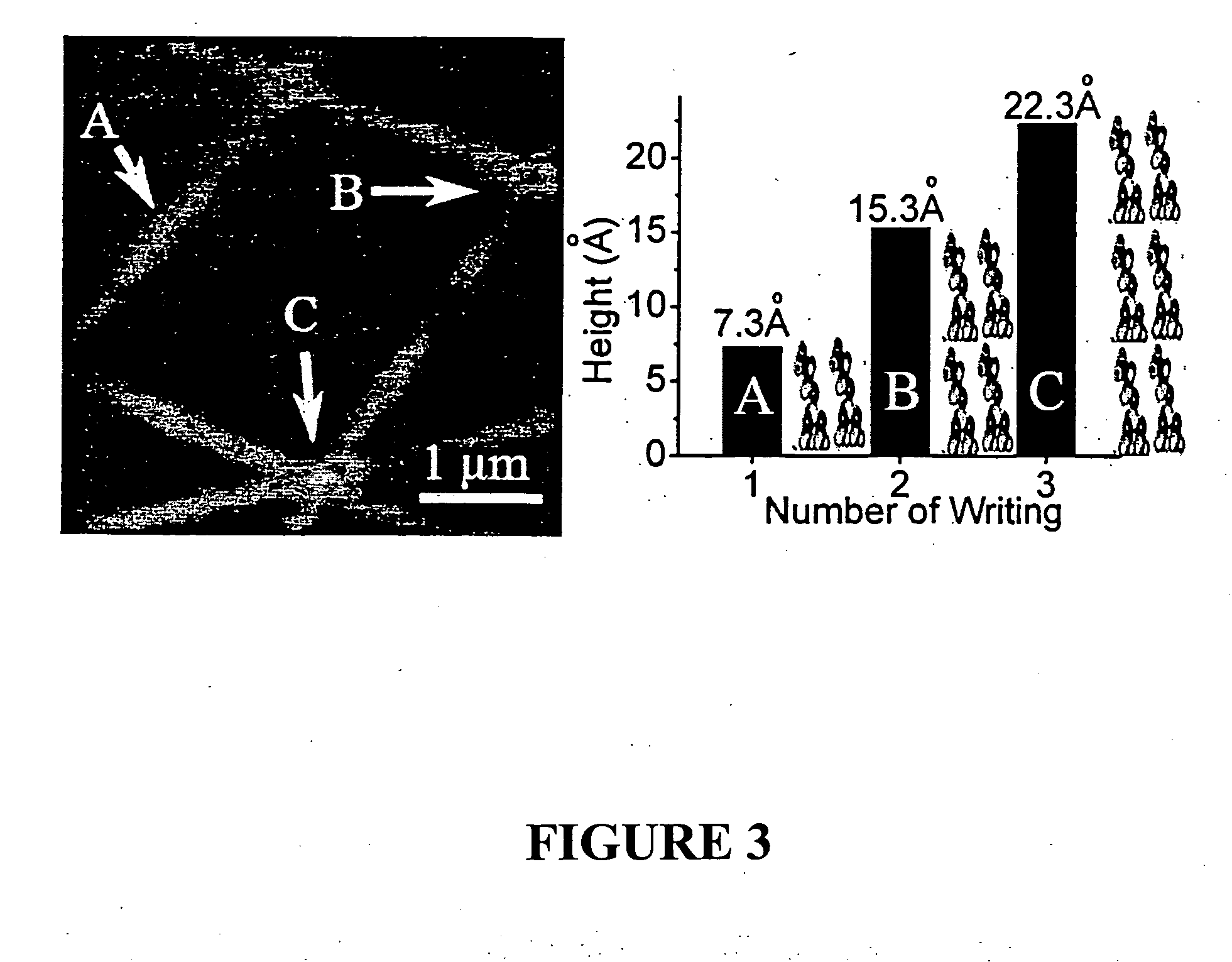
[0236]FIG. 3(a) shows a pattern that has several lines of MPTMS patterning molecules across each other written onto an OTS surface. The pattern has a scan area of 4216×4216 nm. Point A is a point on the MPTMS line. Point B is on an intersection of two MPTMS lines, i.e., where the tip wrote twice. Point C is on an intersection of three MPTMS lines, i.e., where the tip wrote three times. FIG. 3(b) shows the heights of point A, B and C. As shown, the heights of A, B and C closely correspond to the heights of one, two and three layers of MPTMS molecules. This fact indicates that each time the tip writes over the same location, it adds another layer of the ink.
FIG. 4: Fabrication of a Patterned Surface with Two Different Chemistries
[0237] Shown in FIG. 4 are two spots having two different chemistries and fabricated with the same tip in situ. The upper spot, which is a pattern of MPTMS, was fabricated by writing with a tip coated with a very low concentration of MPTMS...
PUM
| Property | Measurement | Unit |
|---|---|---|
| negative voltage bias | aaaaa | aaaaa |
| negative voltage bias | aaaaa | aaaaa |
| humidity | aaaaa | aaaaa |
Abstract
Description
Claims
Application Information
 - R&D
- Intellectual Property
- Life Sciences
- Materials
- Tech Scout
- Unparalleled Data Quality
- Higher Quality Content
- 60% Fewer Hallucinations
Browse by: Latest US Patents, China's latest patents, Technical Efficacy Thesaurus, Application Domain, Technology Topic, Popular Technical Reports.
© 2025 PatSnap. All rights reserved.Legal|Privacy policy|Modern Slavery Act Transparency Statement|Sitemap|About US| Contact US: help@patsnap.com