Method of disposing dummy pattern
a dummy pattern and pattern technology, applied in the field of dummy pattern disposing, can solve the problems of voltage noise, uneven surface of interlayer insulation film,
- Summary
- Abstract
- Description
- Claims
- Application Information
AI Technical Summary
Benefits of technology
Problems solved by technology
Method used
Image

Examples
first embodiment
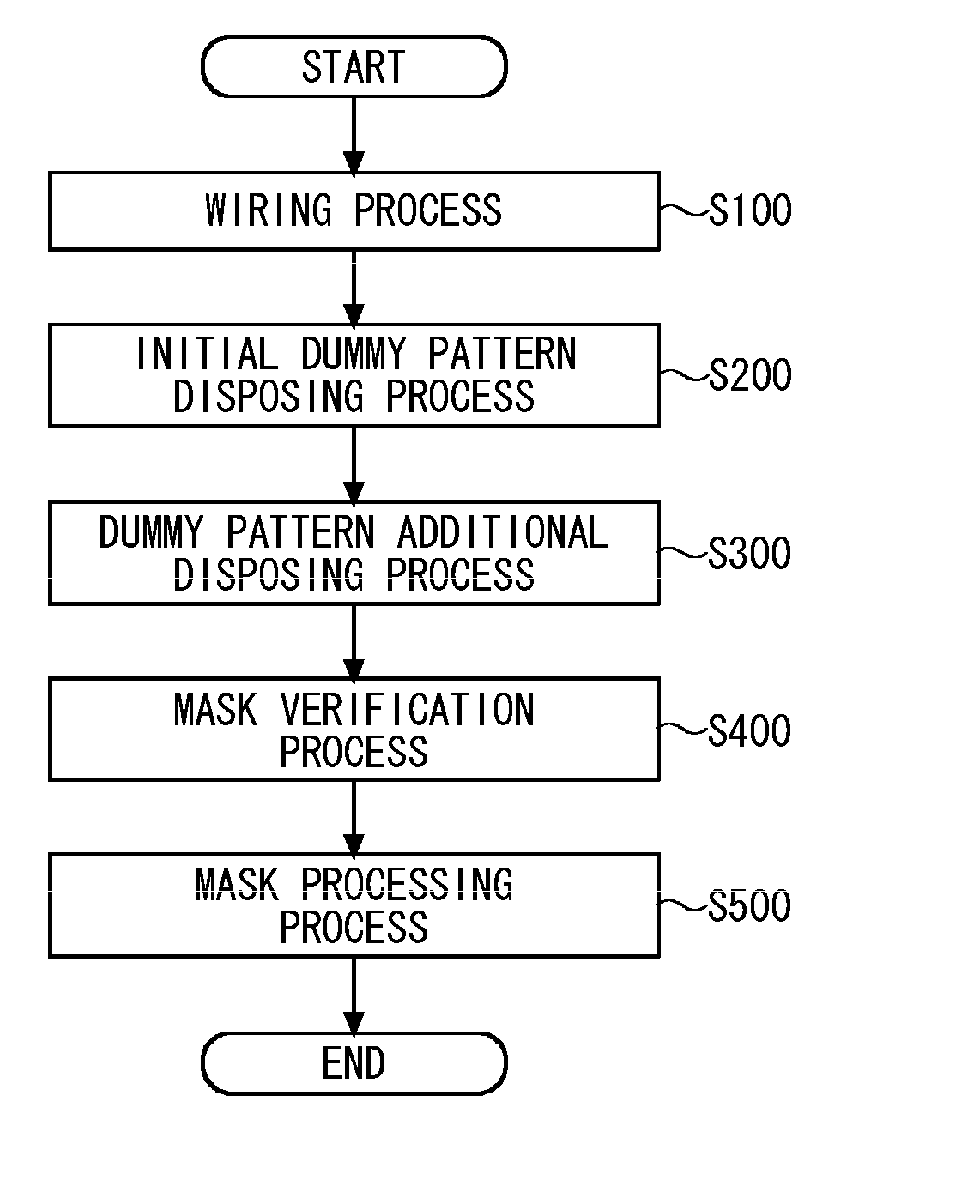
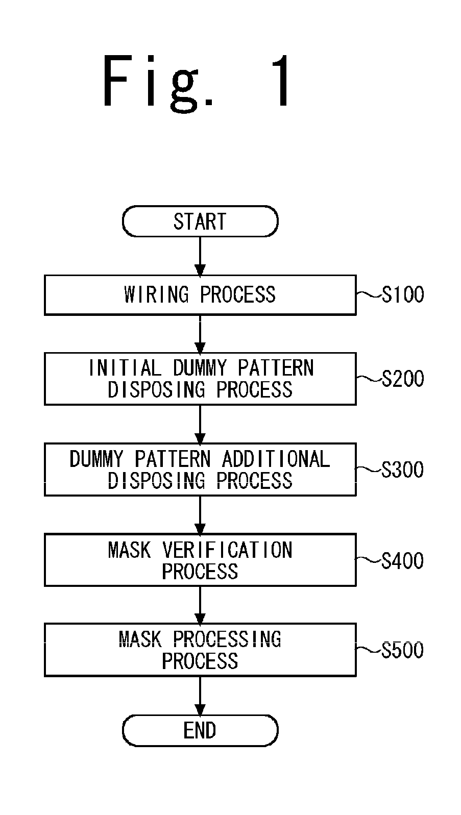
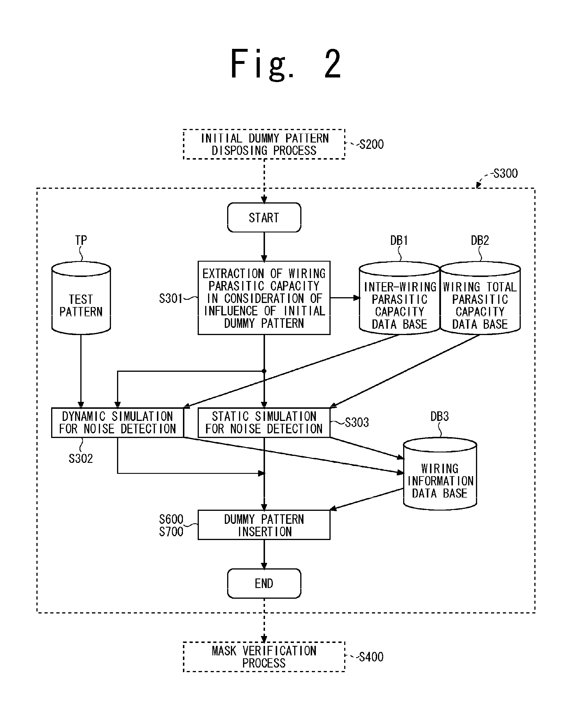
[0038]FIG. 1 is a flow chart showing an example of a layout process of a semiconductor integrated circuit using a dummy pattern disposing method according to a first embodiment of the present invention. The layout process of FIG. 1 includes a wiring process S100, an initial dummy pattern disposing process S200, a dummy pattern additional disposing process S300, a mask verification process S400 and a mask processing process S500. The dummy pattern disposing method of the present invention is executed at the additional dummy pattern disposing process S300, and it will be described in more detail below.
[0039] In the wiring process S100, various functional blocks that are the constituents of the semiconductor integrated circuit are disposed at predetermined positions and are mutually connected to each other by wiring layers. In addition, in the wiring process S100, capacity extraction is performed with respect to each wire, and using the result of the capacity extraction, a post layout...
second embodiment
[0061] In this embodiment, a layout process of a semiconductor integrated circuit using a dummy pattern disposing method is the same as the layout process shown in FIG. 1 in the first embodiment of the present invention. Also, with respect to a dummy pattern disposing process in this embodiment, a basic flow is the same as the dummy pattern disposing process shown in FIG. 2 in the first embodiment of the present invention. In addition, in this embodiment, in the dummy pattern additional disposing process S300 shown in FIG. 2, a dummy pattern insertion process S700 (which will be described below) is implemented instead of the dummy pattern insertion process S600 in the first embodiment. In the following, the details of the dummy pattern insertion process S700 will be described.
[0062]FIG. 10 is a flow chart showing a detailed process flow of the dummy pattern insertion process S700.
[0063] In step S701, analysis of the wiring structure is done using the wiring information data base D...
third embodiment
[0074]FIG. 15 is a flow chart showing an example of a layout process of a semiconductor integrated circuit using a dummy pattern disposing method according to a third embodiment of the present invention. In addition, in this embodiment, in this embodiment, instead of the dummy pattern additional insertion process S300 in the dummy pattern disposing method in the first and second embodiments shown in FIG. 1, a dummy pattern deleting / additional disposing process S800 (which will be described below) is implemented. The rest of the structure of the layout process according to the third embodiment of the present invention is the same as the first or second embodiment, and as for the structure elements that are the same as the first and second embodiments, the same reference numbers will be used, and redundant explanation of those structure elements will be omitted. In the following, details of the dummy pattern insertion process S700 will be described.
[0075]FIG. 16 is a flow chart showi...
PUM
 Abstract
Description
Claims
Application Information
 - R&D
- Intellectual Property
- Life Sciences
- Materials
- Tech Scout
- Unparalleled Data Quality
- Higher Quality Content
- 60% Fewer Hallucinations
Browse by: Latest US Patents, China's latest patents, Technical Efficacy Thesaurus, Application Domain, Technology Topic, Popular Technical Reports.
© 2025 PatSnap. All rights reserved.Legal|Privacy policy|Modern Slavery Act Transparency Statement|Sitemap|About US| Contact US: help@patsnap.com