
Organic light emitting display (OLED) and method of fabricating the same

a light-emitting diode and organic technology, applied in the field of flat panel display, can solve the problems of reducing light-emitting efficiency, affecting the appearance of light-emitting diodes, and affecting the life of the electrode, so as to improve the surface characteristics of the electrode pattern

Inactive Publication Date: 2006-08-17
SAMSUNG MOBILE DISPLAY CO LTD
View PDF6 Cites 23 Cited by
  • Summary
  • Abstract
  • Description
  • Claims
  • Application Information

AI Technical Summary

Benefits of technology

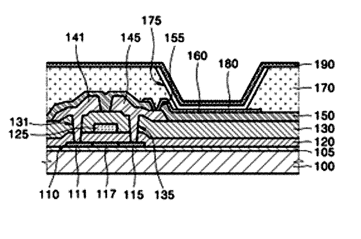
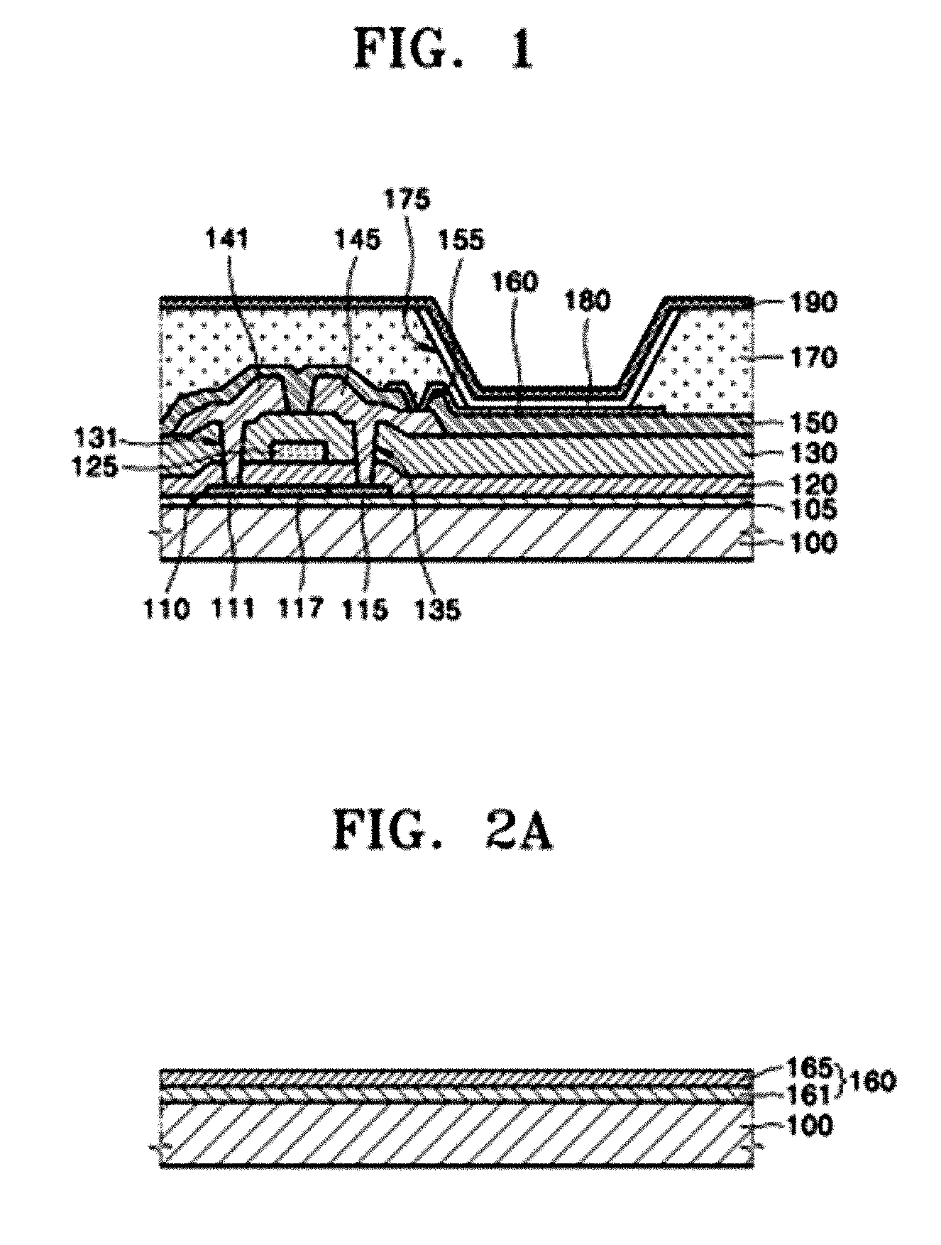
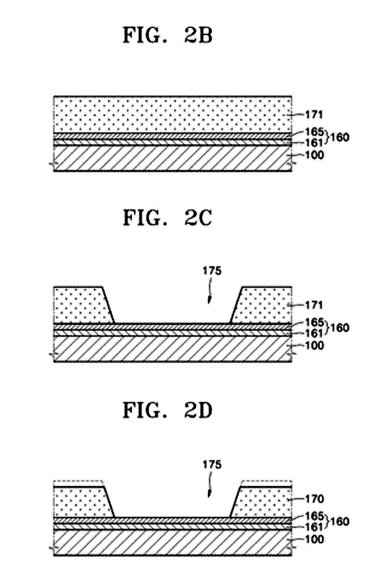
[0015] One embodiment of the present invention is a method of forming an electrode of a flat panel display. The method includes: forming an electrode material on a substrate; patterning the electrode material to form an electrode pattern; forming an insulating layer having a deposition thickness on the substrate; etching the insulating layer to expose a portion of the electrode pattern; and performing a surface treatment process under the condition that the insulating layer is etched by a predetermined thickness from the deposition thickness to improve surface characteristics of the electrode pattern.

Problems solved by technology

As a result, defects such as dark spots may occur and problems may occur, including (1) decreasing light-emitting efficiency and (2) decreasing lifetime.

Method used


Image

  • Organic light emitting display (OLED) and method of fabricating the same
  • Organic light emitting display (OLED) and method of fabricating the same
  • Organic light emitting display (OLED) and method of fabricating the same

Examples


Embodiment Construction

CROSS-REFERENCE TO RELATED APPLICATIONS

[0001] This application claims the benefit of Korean Patent Application No. 10-2005-0011407, filed on February 7, 2005, in the Korean Intellectual Property Office, the disclosure of which is incorporated herein in its entirety by reference.

BACKGROUND OF THE INVENTION

[0002] 1. Field of the Invention

[0003] The present invention relates to a flat panel display and more particularly, to an organic light emitting diode (OLED) display for improving characteristics of indium-tin-oxide (ITO) for use in a pixel electrode by performing surface treatment after forming a pixel separation layer, but before depositing an organic layer. The present invention also relates to a method of fabricating the same.

[0004] 2. Description of the Related Art

[0005] In general, an active matrix organic light emitting diode display includes a plurality of pixels on a substrate, wherein each pixel includes at least one switching thin film transistor, one drive thin film ...


PUM


Abstract

Abstract of the DisclosureAn organic light emitting diode (OLED) display for improving surface characteristics of an indium-tin-oxide (ITO) layer for use as a pixel electrode by performing a surface treatment process after forming a pixel separation layer and before depositing an organic layer and a method of fabricating the same. The method of forming an electrode of a flat panel display includes forming an electrode material on a substrate; patterning the electrode material to form an electrode pattern; forming an insulating layer with a deposition thickness on the substrate; etching the insulating layer to expose a portion of the electrode pattern; and performing a surface treatment process under the condition that the insulating layer is etched by a predetermined thickness from the deposition thickness.

Description

Detailed Description of the InventionCROSS-REFERENCE TO RELATED APPLICATIONS[0001] This application claims the benefit of Korean Patent Application No. 10-2005-0011407, filed on February 7, 2005, in the Korean Intellectual Property Office, the disclosure of which is incorporated herein in its entirety by reference.BACKGROUND OF THE INVENTION[0002] 1. Field of the Invention[0003] The present invention relates to a flat panel display and more particularly, to an organic light emitting diode (OLED) display for improving characteristics of indium-tin-oxide (ITO) for use in a pixel electrode by performing surface treatment after forming a pixel separation layer, but before depositing an organic layer. The present invention also relates to a method of fabricating the same.[0004] 2. Description of the Related Art[0005] In general, an active matrix organic light emitting diode display includes a plurality of pixels on a substrate, wherein each pixel includes at least one switching thin ...

Claims


Application Information

Patent Timeline
IPC IPC(8): H01J9/24H01J9/00
CPCH01L27/3244H01L27/3246H01L51/5206H01L51/56H10K59/122H10K71/00H10K59/8051B42F5/00B42D1/08H10K50/81
Inventor KIM, JAE-JUNGPARK, JOON-YOUNGLEE, JEON-YEOLMIN, KYOUNG-WOOK
Owner SAMSUNG MOBILE DISPLAY CO LTD
Learn More