
Method for defining a feature on a substrate

a technology of feature and substrate, applied in the direction of sidewalk paving, instruments, roads, etc., can solve the problems of difficult to meet escalating requirements, new challenges in the manufacture of devices with smaller feature sizes, and copper (cu) presents challenges to precise patterning and etching

Inactive Publication Date: 2006-08-17
VERSUM MATERIALS US LLC
View PDF50 Cites 108 Cited by
  • Summary
  • Abstract
  • Description
  • Claims
  • Application Information

AI Technical Summary

Problems solved by technology

Manufacturing of devices with smaller feature sizes introduces new challenges in many of the processes conventionally used in semiconductor fabrication.
Such escalating requirements have been found difficult to satisfy in terms of providing a low RC (resistance capacitance) interconnect pattern, particularly where sub-micron via contacts and trenches have high aspect ratios imposed by miniaturization.
Copper (Cu), however, presents challenges to precise patterning and etching.
For example, Cu does not readily form volatile chlorides or fluorides, rendering typical plasma etching based upon chlorine and / or fluorine chemistries impractically slow.
Problems can occur in the patterning and the fabrication of features in ICs as a result of reflection of the exposing radiation from the surface (or surfaces) lying below the layer of photoresist.
For example, interferences of incident and reflected radiation occurring within the layer of photoresist lead to non-uniform photoresist exposure and imprecise patterning.
In addition, exposing radiation can reflect from surface topography or regions of non-uniform reflectivity resulting in exposure of photoresist in regions lying beneath the photomask and for which exposure is not desired.
In both cases, variations in the feature critical dimensions (“CDs”) can occur, adding to the challenges of precise and reproducible fabrication of IC features.
In addition, BARC layers may be designed through choice of BARC material and thickness such that, at the wavelength of the exposing radiation, destructive interference occurs between incident and reflected radiation.
The use of porous dielectric materials with a SLAM (which includes BARC materials), has given rise to other problems.
For example, an issue with using porous dielectric layers relative to dense dielectric materials currently used in the art is that dry etch rates and chemical compatability will depend upon material properties such that the etch rate selectivities for a porous dielectric and the current art SLAM are not properly balanced.

Method used


Image

  • Method for defining a feature on a substrate
  • Method for defining a feature on a substrate
  • Method for defining a feature on a substrate

Examples


examples

[0077] In examples 1-3, the thickness and refractive index of each film were measured on an SCI Filmtek 2000 Reflectometer. Dielectric constants were determined using Hg probe technique on low resistivity p-type wafers (<0.02 ohm-cm). Mechanical properties were determined using MTS Nano Indenter.

[0078] In some of the following examples, UV exposure was performed using a Fusion UV model F305 ultraviolet lamp. The films subjected to UV exposure were placed in a 2″ diameter quartz glass tube with sealed end caps. In examples involving a vacuum or inert atmospheres, three pump and purge cycles were performed prior to UV exposure to ensure that any oxygen present was removed from the process tube. Exposure times varied between 0 and 30 minutes.

[0079] In examples 4-5, the thickness of each film were determined by spectroscopic ellipsometry using a variable angle spectroscopic ellipsometer, Model SE 800 manufactured by Sentech Instruments GmbH, and calculated by SpectraRay software. The ...

examples 1 , 2

Examples 1, 2, and 3

PECVD Deposited Films

[0080] Exemplary PECVD films were deposited using an Applied Materials Precision-5000 system in a 200 mm DxZ vacuum chamber that was fitted with an Advance Energy 200 rf generator and using an undoped TEOS process kit. The PECVD process involved the following basic steps: initial set-up and stabilization of gas flows deposition, and purge / evacuation of chamber prior to wafer removal. Exemplary films 1 were deposited using the precursor diethoxymethylsilane (DEMS) with carbon dioxide as carrier gas. Exemplary films 2 were deposited using the precursors DEMS and alphaterpinene (ATP) as the porogen along with carbon dioxide as carrier gas. In Exemplary films 3, the as-deposited films containing DEMS and ATP was exposed to UV light at a pressure of less than 1 torr for 10 minutes to at least partially remove the ATP contained therein. The temperature of the film reached approximately 400° C. during the exposure.

example 4

Spin-On Deposited Films with Dielectric Constant of Approximately 2.2

[0081] Silica sources 22.5 g of tetraethylorthosilicate (TEOS) and 22.5 g of methytriethoxysilane (MTES) are mixed together. 100 g of propylene glycol propyl ether (PGPE) and 9.7 g of Triton X-114 are added to the silica source and mixed thoroughly. In a separate container, 24 g of 0.1 M nitric acid (HNO3) and 1 g of 2.4 wt % tetramethylammonium hydroxide (TMAH) are combined and mixed thoroughly. While the silica source solution is mixing, the HNO3 / TMAH solution is added. The entire solution is mixed for 1 hour. Typically, the solution is then aged at room temperature for one day before the solution is filtered through a 0.2 micron Teflon filter. The solution is then deposited onto a Si wafer spinning at 500 rpm for 7 seconds followed by accleration to 1800 rpm for 40 seconds. The film prepared via this method is then cured in air at 90° C. for 90 seconds, 180° C. for 90 seconds, and 400° C. for 3 minutes.


PUM

PropertyMeasurementUnit
wavelengthsaaaaaaaaaa

Abstract

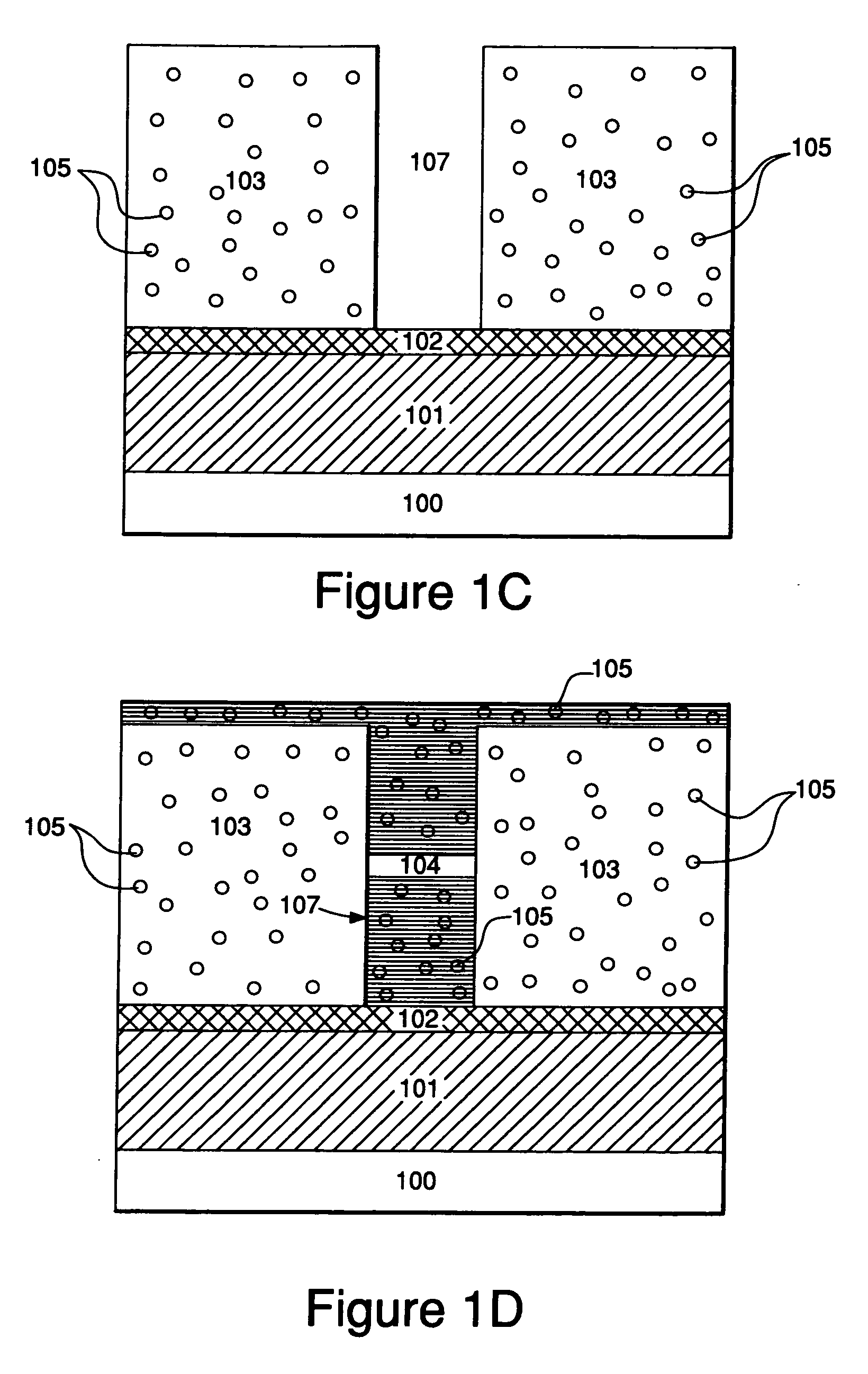
An improved method of forming a feature in a semiconductor substrate is described. The method comprises the steps of forming a porous dielectric layer on a substrate; removing a first portion of the porous dielectric layer to form a first etched region; filling the first etched region with a porous sacrificial light absorbing material having dry etch properties similar to those of the porous dielectric layer; removing a portion of the porous sacrificial light absorbing material and a second portion of the porous dielectric layer to form a second etched region; and removing the remaining portions of the porous sacrificial light absorbing material by employing a process, wherein the porous sacrificial light absorbing material has an etch rate greater than that of the porous dielectric layer in the process.

Description

CROSS-REFERENCE TO RELATED APPLICATIONS [0001] This application claims the benefit of priority under 35 U.S.C. § 119(e) to earlier filed U.S. patent application Ser. No. 60 / 652,875, filed on Feb. 15, 2005, the disclosure of which is incorporated by reference in its entirety.BACKGROUND OF THE INVENTION [0002] The present invention relates to a method for making a semiconductor device. [0003] To meet the requirements for faster performance, the characteristic dimensions of features of integrated circuit devices have continued to be decreased. Manufacturing of devices with smaller feature sizes introduces new challenges in many of the processes conventionally used in semiconductor fabrication. The escalating requirements for high-density and performance associated with ultra large-scale integration semiconductor wiring require responsive changes in interconnect technology. Such escalating requirements have been found difficult to satisfy in terms of providing a low RC (resistance capac...

Claims


Application Information

Patent Timeline
Patent Type & Authority Applications(United States)
IPC IPC(8): G03C5/00C23C16/24
CPCH01L21/02126H01L21/02203H01L21/02216H01L21/02274H01L21/02282H01L21/02304H01L21/02348H01L21/02362H01L21/31111H01L21/31116H01L21/31144H01L21/3121H01L21/31695H01L21/76808H01L21/7682H01L21/76826H01L2221/1047A61H3/066E01C15/00
Inventor O'NEILL, MARK LEONARDWEIGEL, SCOTT JEFFREYRENNIE, DAVID BARRYROBERTS, DAVID ALLENKARWACKI, EUGENE JOSEPH JR.MAC DOUGALL, JAMES EDWARD
Owner VERSUM MATERIALS US LLC
Learn More