Method for producing group III nitride single crystal and apparatus used therefor
a technology of group iii and nitride, which is applied in the direction of crystal growth process, polycrystalline material growth, pressurized chemical process, etc., can solve the problems of difficult to improve the quality of crystals to be obtained, non-uniform nitrogen distribution, and low growth rate, so as to achieve uniform thickness, reduce dislocation density, and produce quickly
- Summary
- Abstract
- Description
- Claims
- Application Information
AI Technical Summary
Benefits of technology
Problems solved by technology
Method used
Image
Examples
example 1
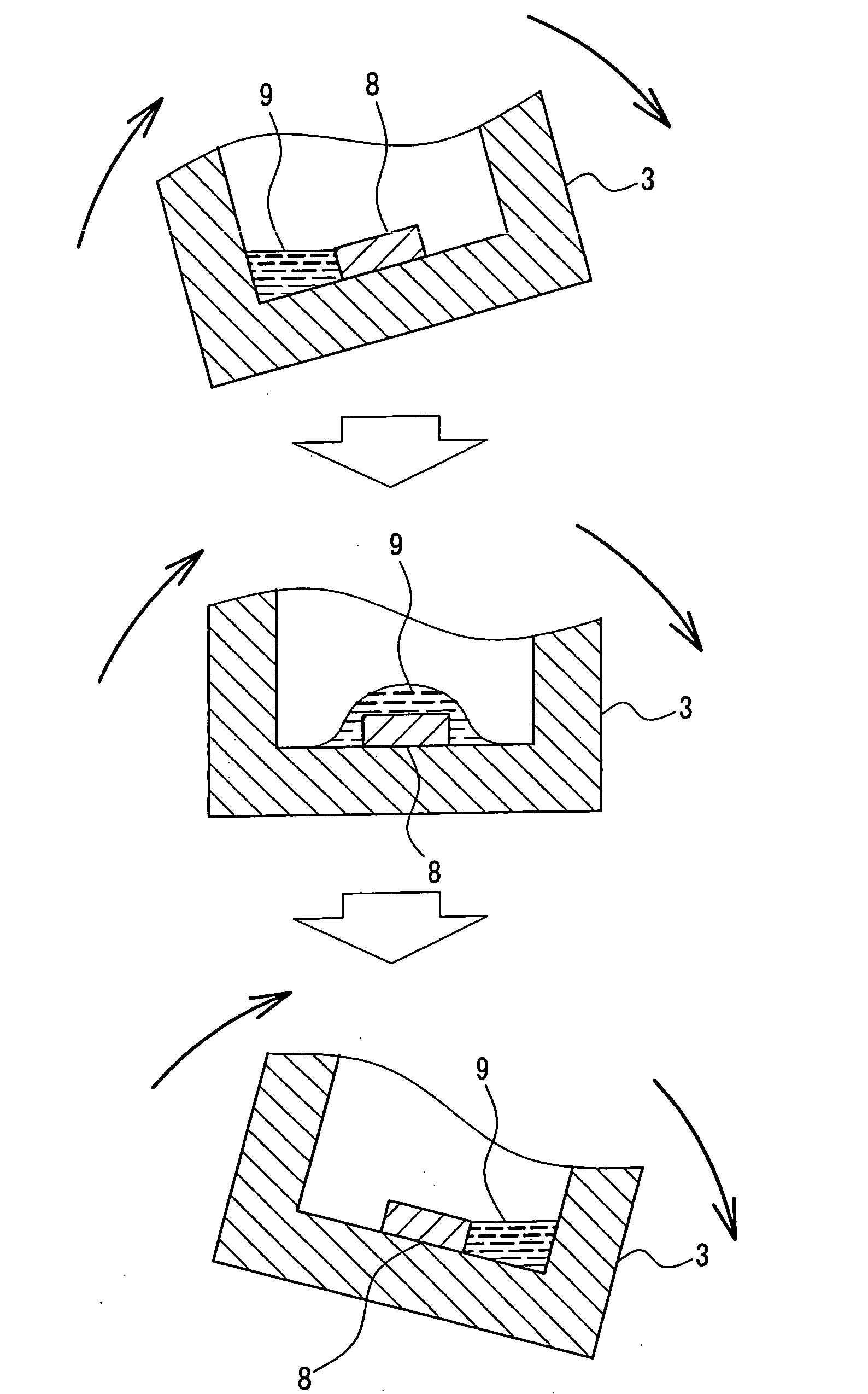
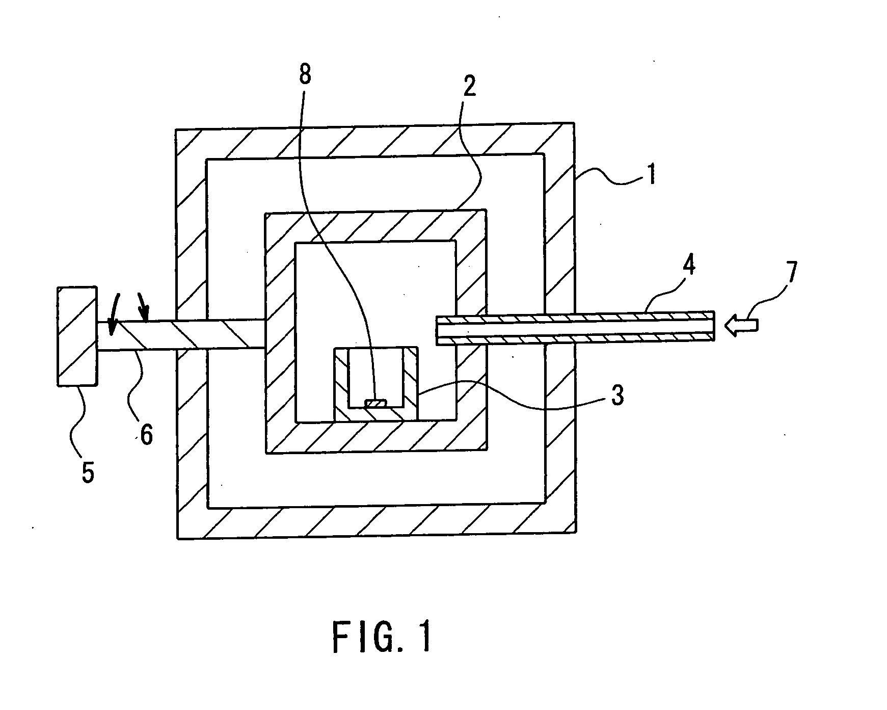
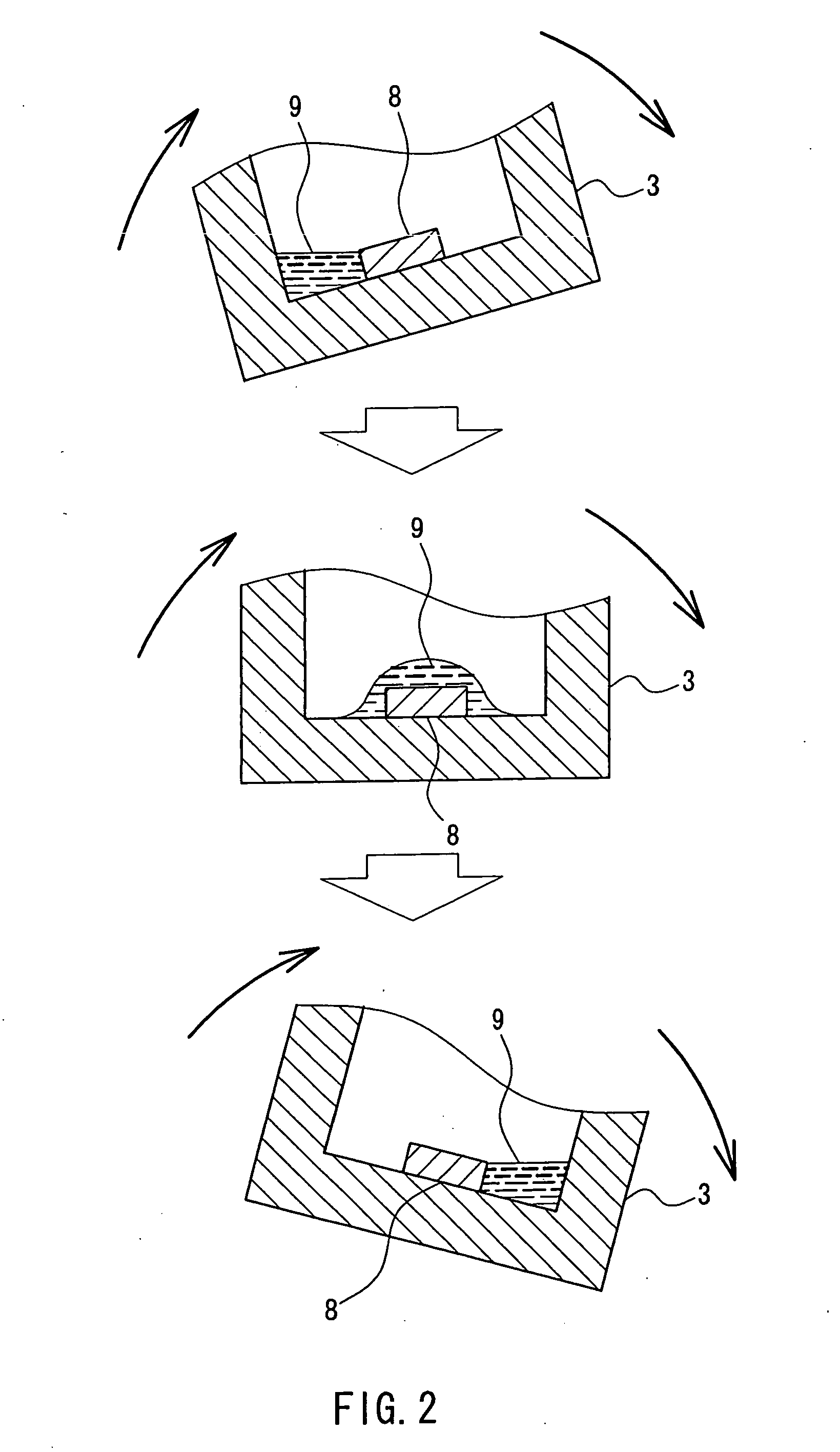
[0044] Gallium nitride single crystals were produced using the apparatus shown in FIG. 1. First, GaN thin-film crystals were formed on the surface of a sapphire substrate 8 by the MOCVD method. The substrate 8 was placed at one end (in this example, the “end” refers to a part that moves up and down when the reaction vessel is rocked) of the reaction vessel. The boron nitride reaction vessel 3 in which 2.0 g of gallium and 5.77 g of flux material (sodium) had been put was placed in the heating container 2. The temperature thereof was raised to a growth temperature of 890° C. While the temperature was raised, nitrogen gas 7 was fed into the heating container 2 through the pipe 4 to increase the pressure to a predetermined pressure. In this case, until the heating container 2 was heated to the predetermined temperature, the substrate 8 was prevented from coming into contact with the flux, with the reaction vessel 3 being tilted. The flux component was sodium only. The growth conditions...
example 2
[0045] Gallium nitride single crystals were produced using the apparatus shown in FIG. 1. First, a 3-μm thick GaN film was formed on a sapphire substrate 8 by the MOCVD method. This substrate 8 was placed on one side on the bottom of the boron nitride reaction vessel 3. Then 3.0 g of gallium and a flux material (8.78 g of sodium and 0.027 g of lithium (sodium:lithium=99:1 (mol))) were put into the reaction vessel 3. This reaction vessel 3 was set in the heating container 2. The reaction vessel 3 was tilted in a certain direction to prevent the substrate surface from coming into contact with the raw material. Thereafter, nitrogen gas was fed to increase the pressure to 10 atm (10×1.013×105 Pa) and then the reaction vessel 3 was heated to 890° C. After the rise in temperature and pressure was completed, the reaction vessel 3 was rocked to allow the raw material solution to flow from side to side and thereby to allow the surface of the GaN substrate to be covered continuously with a th...
example 3
[0046] In this example, GaN single crystals were produced while the lower part of the reaction vessel was heated, which generated heat convection and thereby stirred a Na flux and Ga to mix them together, using the apparatus shown in FIGS. 6 and 7. As shown in FIG. 6, this apparatus includes a gas cylinder 11, an electric furnace 14, and a heat- and pressure-resistant container 13 placed in the electric furnace 14. A pipe 21 is connected to the gas cylinder 11 and is provided with a gas pressure controller 15 and a pressure control valve 25. A leak pipe is attached to a middle part of the pipe 21 and a leak valve 24 is disposed at the end of the leak pipe. The pipe 21 is connected to a pipe 22 that is connected to a pipe 23. The pipe 23 enters the electric furnace 14 and is connected to the heat- and pressure-resistant container 13. An electric heater 18 is attached to the outer wall of the lower part of the heat- and pressure-resistant container 13. As shown in FIG. 7, a reaction v...
PUM
| Property | Measurement | Unit |
|---|---|---|
| pressure | aaaaa | aaaaa |
| temperature | aaaaa | aaaaa |
| diameter | aaaaa | aaaaa |
Abstract
Description
Claims
Application Information
 - R&D
- Intellectual Property
- Life Sciences
- Materials
- Tech Scout
- Unparalleled Data Quality
- Higher Quality Content
- 60% Fewer Hallucinations
Browse by: Latest US Patents, China's latest patents, Technical Efficacy Thesaurus, Application Domain, Technology Topic, Popular Technical Reports.
© 2025 PatSnap. All rights reserved.Legal|Privacy policy|Modern Slavery Act Transparency Statement|Sitemap|About US| Contact US: help@patsnap.com


