
Method for manufacturing semiconductor device

Inactive Publication Date: 2006-07-27
FUJI ELECTRIC CO LTD
View PDF10 Cites 63 Cited by
  • Summary
  • Abstract
  • Description
  • Claims
  • Application Information

AI Technical Summary

Benefits of technology

[0022] partially removing the portion of the gate insulator film on the sidewall of the trench near the aperture thereof to selectively reduce the thickness of that portion of the gate insulator film.
[0023] Since a thick oxide film is formed relatively easily in the bottom of a trench or in or in both the bottom of a trench and on the sidewall of the trench near the bottom thereof, trench MOSFETs exhibiting a high breakdown voltage and trench IGBTs exhibiting a high breakdown voltage can be manufactured by the method of the invention.

Problems solved by technology

Although semiconductor apparatuses integrating power MOS devices for the switching devices thereof are used for switching power supply ICs and driver ICs mounted on hand held electronic equipment and data communication equipment, on-resistance reduction and switching characteristics improvement for the power MOS devices pose problems which should be obviated.
If nitrogen is doped locally in the trench sidewall, the device characteristics will be impaired due to a reduction of carrier mobility, stress generation and other such causes.
However, several adverse effects will occur, including for example, (1) the characteristics and reliability of the device will be impaired by the residual nitrogen, (2) crystal defects and stress will be caused by the oxidation, (3) the characteristics and the reliability of the device will be impaired also by stress resulting from formation of a bird's beak.
When a silicon wafer, into which argon ions are implanted, is treated thermally, the argon gas condenses in the silicon wafer during the heat treatment, causing vacancy-type defects called “micro bubbles.” The micro bubbles are liable to adsorb heavy metals, impairing the device characteristics.
Thus, the micro bubbles also cause a troublesome reduction in carrier mobility.

Method used


Image

  • Method for manufacturing semiconductor device
  • Method for manufacturing semiconductor device
  • Method for manufacturing semiconductor device

Examples


Embodiment Construction

[0035] Now the invention will be described in detail hereinafter with reference to the accompanied drawing figures, which illustrate the preferred embodiments of the invention.

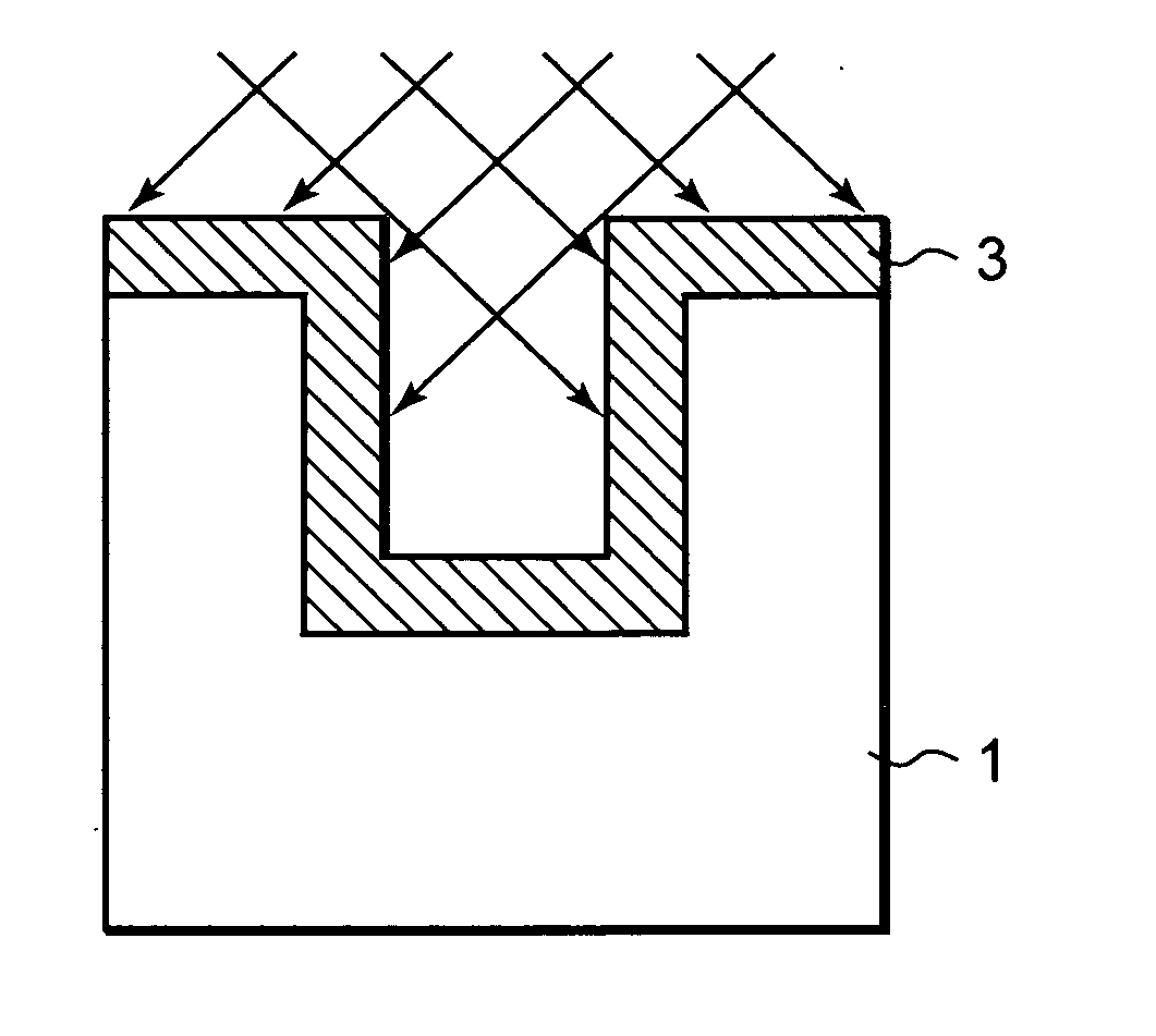
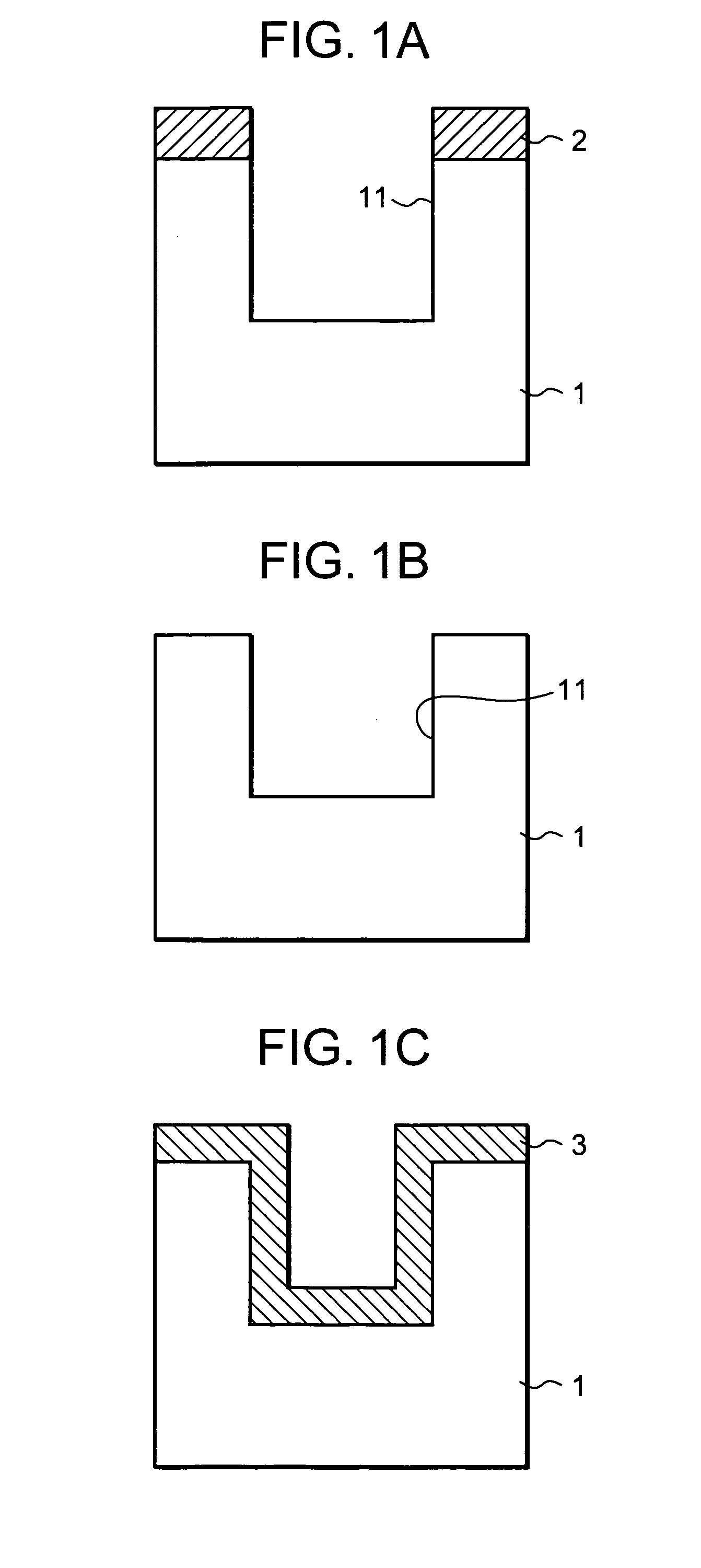
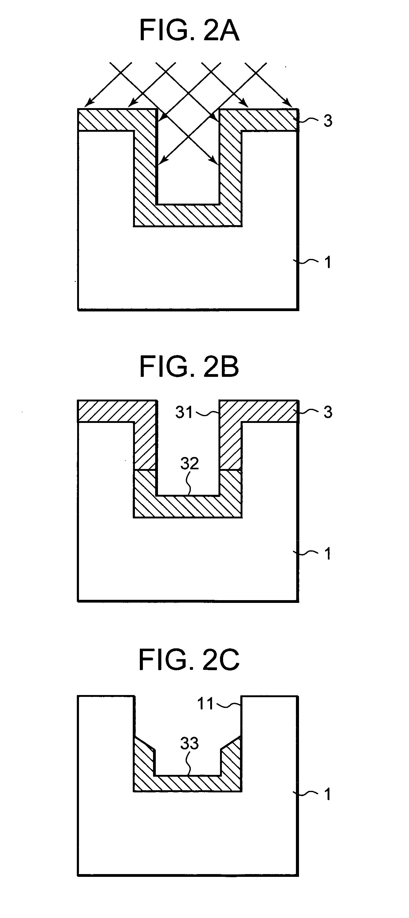
[0036]FIGS. 1A through 1C are cross-sectional views describing the steps for manufacturing a semiconductor device according to the embodiment of the invention. FIGS. 2A through 2C are cross-sectional views describing the steps, subsequent to the steps described in FIGS. 1A through 1C, for manufacturing the semiconductor device according to the embodiment of the invention.

[0037] Referring now to FIG. 1A, an etching mask 2 is formed on a semiconductor substrate 1 such as a silicon wafer. Then, a trench 11 having a predetermined width and a predetermined depth is formed by etching semiconductor substrate 1. Etching mask 2 is a silicon oxide film or a silicon nitride film shaped by a photoresist with a predetermined shape (the step (a)). Referring now to FIG. 1B, the silicon oxide film used for mask 2 is removed...


PUM


Abstract

The method for manufacturing a semiconductor device according to the invention includes forming a thick silicon oxide film uniformly in a trench. Argon ions or the like implanted obliquely into the trench to form an ion implanted damaged region selectively in the portion of the silicon oxide film on the trench sidewall utilizing the shadowing effects of the oblique ion implantation. The silicon oxide film is wet etched to selectively remove the silicon oxide film in the ion implanted damaged region utilizing the etching rate difference, wherein the etching rate is faster in the damaged region than in the undamaged region. As a result, a thick residual oxide film is formed on the bottom and the lower sidewall portion of the trenchwithout causing any bird's beak.

Description

CROSS-REFERENCE TO RELATED APPLICATION [0001] This application claims foreign priority benefits under 35 USC 119 of Japanese Patent Application Serial No. 2005-013588, the entire disclosure of which is incorporated herein by reference. FIELD OF THE INVENTION [0002] The invention relates to a method for manufacturing a semiconductor device that includes a trench-type device having a semiconductor substrate, trenches formed in the substrate, and gate insulator layers formed on the bottom and the sidewall of the trenches. Specifically, the invention relates to a method for forming a thick oxide film on some areas in the trench in manufacturing trench-type semiconductor devices, having the gates thereof in the trenches, such as metal oxide semiconductor field effect transistors (hereinafter referred to as “MOSFETs”), insulated gate bipolar transistors (hereinafter referred to as “IGBTs”) and such trench MOS devices. BACKGROUND OF THE INVENTION [0003] Although semiconductor apparatuses i...

Claims


Application Information

Patent Timeline
IPC IPC(8): H01L21/338
CPCH01L21/26586H01L21/31155H01L29/41766H01L29/4236H01L29/42368H01L29/66621H01L29/66659H01L29/7834H01L29/7835
Inventor SHIMOYAMA, KAZUOKITAMURA, MUTSUMILU, HONGFEI
Owner FUJI ELECTRIC CO LTD
Learn More