Method of producing semiconductor device
a semiconductor device and capac technology, applied in the direction of semiconductor devices, capacitors, electrical equipment, etc., can solve the problems of high cost, difficult to obtain, and difficult to obtain ferroelectric capacitors, and achieve high reliability
- Summary
- Abstract
- Description
- Claims
- Application Information
AI Technical Summary
Benefits of technology
Problems solved by technology
Method used
Image

Examples
example 1
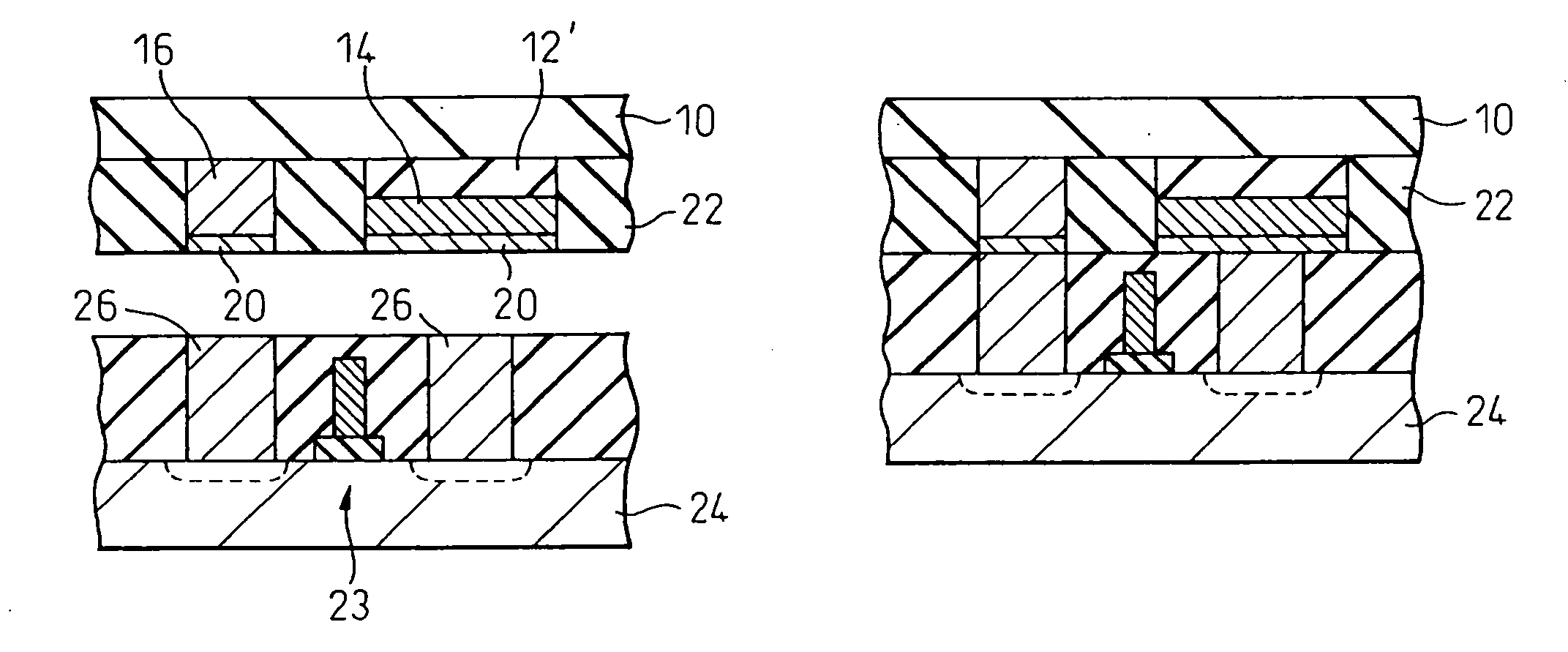
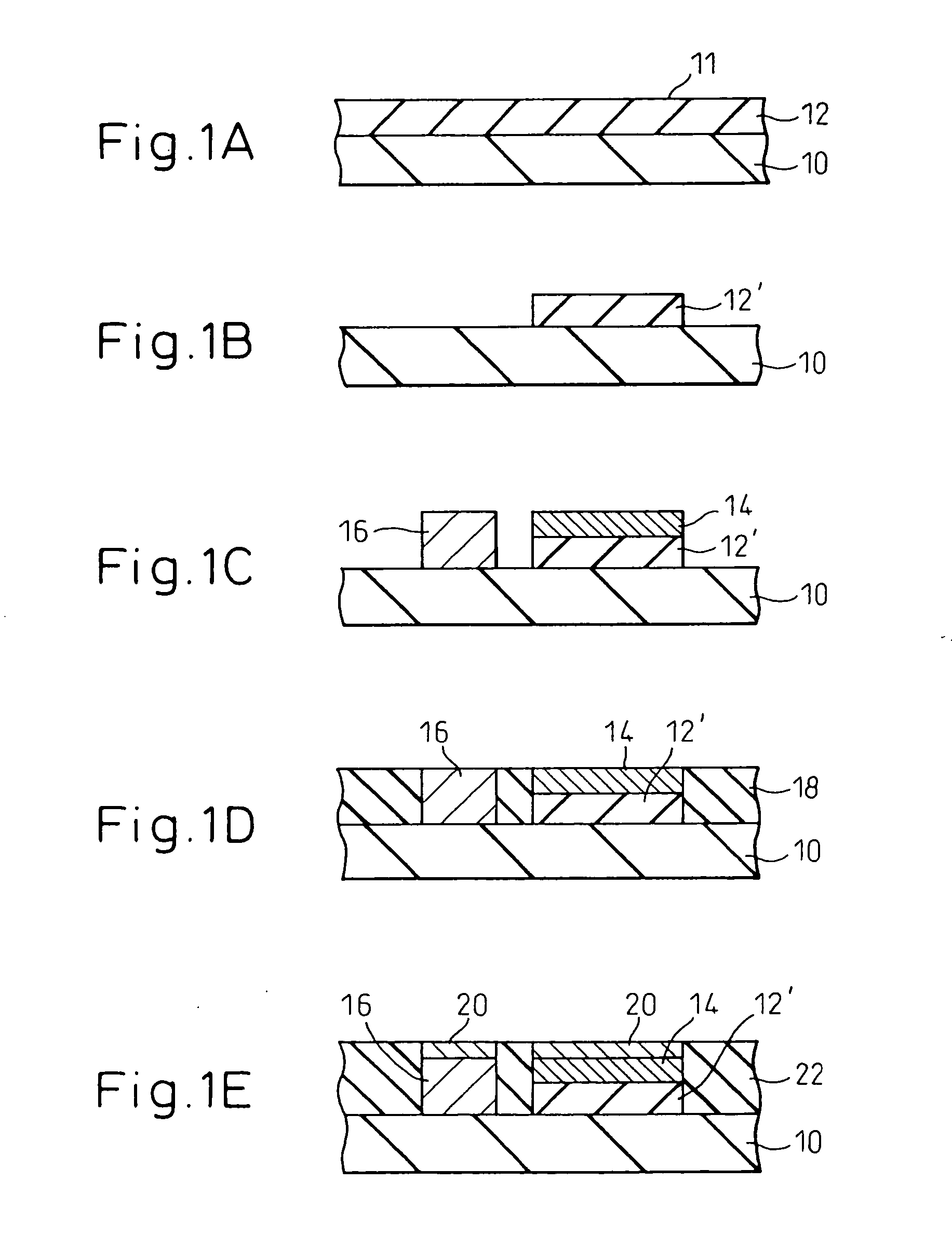
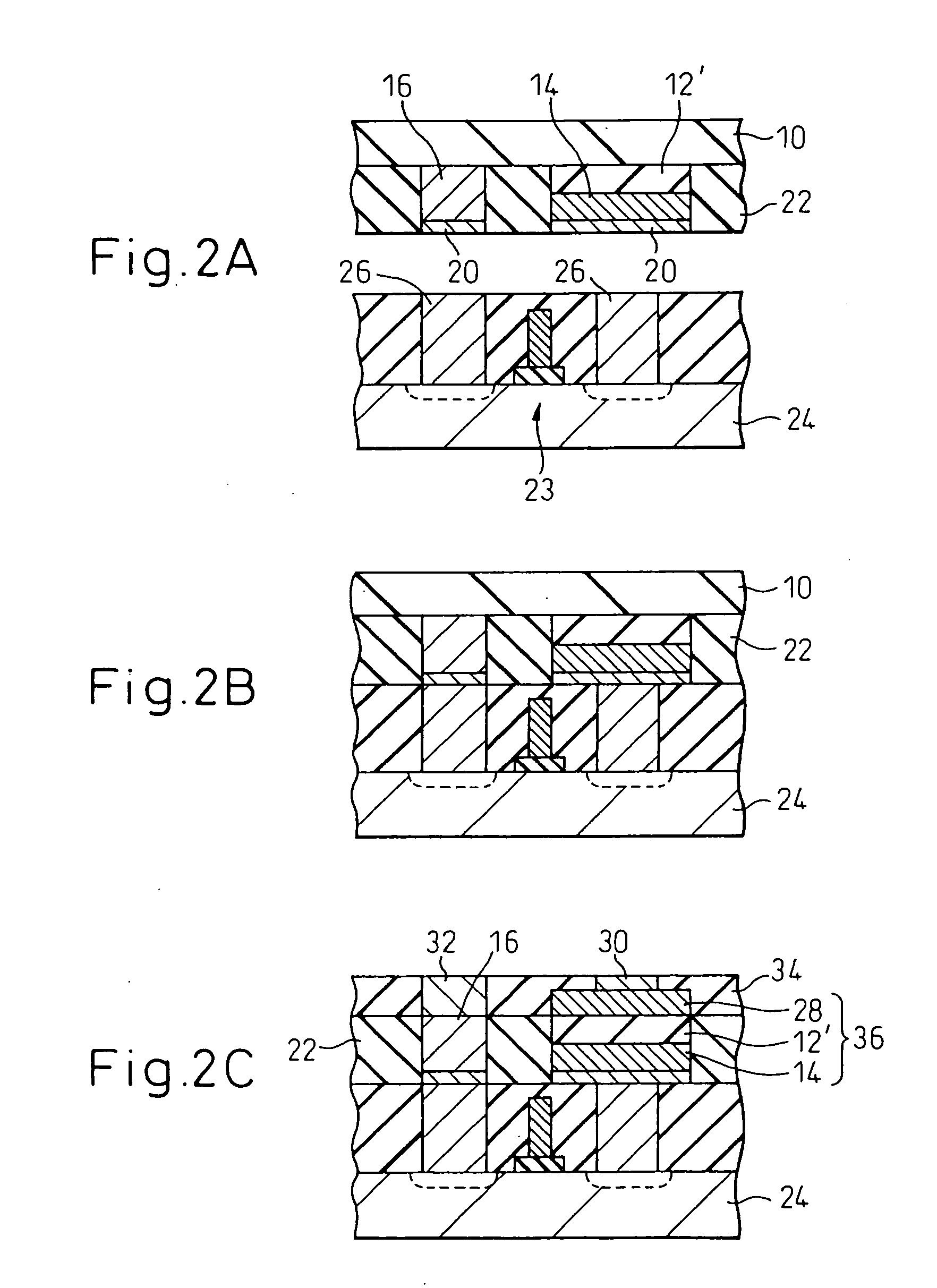
[0038] As shown in FIG. 1A, a single crystalline PZT layer 12 is epitaxially grown on a single crystalline substrate 10, the single crystalline PZT layer 12 having a plane (111) 11 in parallel with the surface of the substrate 10. As the single crystalline substrate 10, there can be used a substrate having, for example, a MgO plane (111), an SrTiO3 plane (111) or an α-Al2O3 plane (0001).
[0039] The single crystalline PZT (111) can be epitaxially grown by an organometal chemical vapor phase deposition (MOCVD) method, a molecular beam epitaxy (MBE) method or a pulse laser deposition (PLD) method. The film-forming methods are not limited thereto. Also, by not being limited to PZT (PbZrxTi1-xO3), there can be used such ferroelectric material as PLZT (PbyLa1-yZrxT1-xO3), PLCSZT ((Pb, La, Ca, Sr)(Zr, Ti)O3), as well as a material derived therefrom by adding Nb thereto.
[0040] For example, the formation of PZT film by the MOCVD method can be carried out by using Pb(THD)2, Zr(THD)4 and Ti(i...
example 2
[0046] This example illustrates the production of a semiconductor device incorporating a ferroelectric capacitor by forming a PZT thin film on the plane (0001) of a sapphire (α-Al2O3) substrate having through holes formed.
[0047] As shown in FIG. 3A, through holes 52a, 52b are perforated in a sapphire (α-Al2O3) single crystalline substrate 50 having a plane (0001) 51 as the upper surface. The through hole 52a is for forming a plug that will connect to one electrode of the capacitor and the through hole 52b is for forming a plug that will serve as an interconnection to be connected to a semiconductor substrate (circuit board) that is to be bonded later. These through holes may be perforated by machining the sapphire substrate 50, or by a dry etching method using a reactive gas or an ionic milling method using Ar ions, or by chemical etching using molten KOH.
[0048] As shown in FIG. 3B, a thin film 54 is formed on the plane (0001) 51 of the substrate 50, the thin film 54 having a plan...
example 3
[0052] This example illustrates the production of a semiconductor device incorporating a ferroelectric capacitor by forming a PZT thin film on the plane (111) of the silicon substrate having through holes formed.
[0053] As shown in FIG. 6A, through holes 92a, 92b are perforated in a silicon substrate 90 having a plane (111) 91 as an upper surface. The through hole 92a is for forming a plug that will connect to one electrode of the capacitor and the through hole 92b is for forming a plug that will serve as an interconnection to be connected to a semiconductor substrate that is to be bonded later. These through holes may be perforated by machining the silicon substrate 90, or by a dry etching method using a reactive gas or an ionic milling method using Ar ions, or by chemical etching using a mixed acid of HF and HNO3.
[0054] As shown in FIG. 6B, a thin MgAl2O4 film 94 is formed on the plane (111) 91 of the substrate 90, the thin film 94 having a plane (111) 95 in parallel with the pla...
PUM
 Abstract
Description
Claims
Application Information
 - R&D
- Intellectual Property
- Life Sciences
- Materials
- Tech Scout
- Unparalleled Data Quality
- Higher Quality Content
- 60% Fewer Hallucinations
Browse by: Latest US Patents, China's latest patents, Technical Efficacy Thesaurus, Application Domain, Technology Topic, Popular Technical Reports.
© 2025 PatSnap. All rights reserved.Legal|Privacy policy|Modern Slavery Act Transparency Statement|Sitemap|About US| Contact US: help@patsnap.com