Frequency doubling of semiconductor lasers to generate 300-600 nm light
a semiconductor laser and frequency doubling technology, applied in semiconductor lasers, laser cooling arrangements, laser details, etc., can solve the problems of gas lasers, inefficient, bulky, etc., and achieve the effect of reducing the number of gas-discharge tubes, and reducing the cost of gas-discharge tubes
- Summary
- Abstract
- Description
- Claims
- Application Information
AI Technical Summary
Problems solved by technology
Method used
Image
Examples
Embodiment Construction
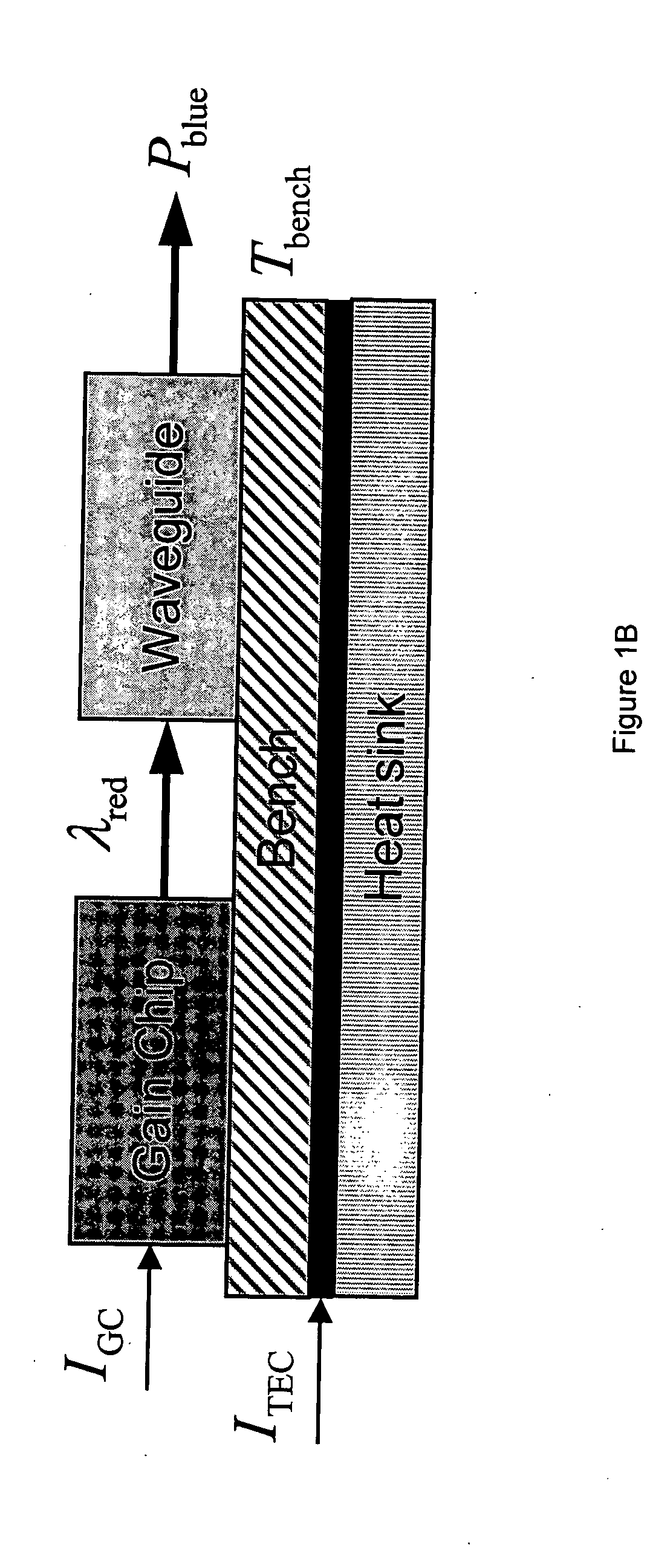
[0023] The optical layout of the laser is shown in FIGS. 1a and 1b. It comprises two building blocks—a pump section, which is preferably an external cavity single frequency semiconductor laser, and a frequency doubling section as shown in FIG. 1a which contains, for example, a periodically poled MgO:LiNbO3(Magnesium Oxide doped Lithium Niobate) ridge waveguide, (manufactured by NGK Insulators, Ltd), with associated focusing and beam shaping optics. The size of the waveguide is 3 by 5 micrometers, respectively in the vertical and horizontal directions and the length is 8.5 mm. The poling period was optimized to have a phase matching temperature of about 26° C. for a fundamental (pump) wavelength of 976 nm.
[0024] The periodically poled ridge waveguide keeps both the fundamental and second harmonic waves confined in two dimensions within substantially the same area. This results in a very high conversion efficiency provided that the pump field is efficiently coupled into the fundament...
PUM
 Abstract
Description
Claims
Application Information
 - R&D
- Intellectual Property
- Life Sciences
- Materials
- Tech Scout
- Unparalleled Data Quality
- Higher Quality Content
- 60% Fewer Hallucinations
Browse by: Latest US Patents, China's latest patents, Technical Efficacy Thesaurus, Application Domain, Technology Topic, Popular Technical Reports.
© 2025 PatSnap. All rights reserved.Legal|Privacy policy|Modern Slavery Act Transparency Statement|Sitemap|About US| Contact US: help@patsnap.com


