Current driver, data driver, and display device

a current driver and data driver technology, applied in the field of current drivers, can solve the problems that the voltage values of bias voltages vbiasa and vbiasb cannot be set at appropriate values

Inactive Publication Date: 2006-06-22
COLLABO INNOVATIONS INC
View PDF13 Cites 7 Cited by
  • Summary
  • Abstract
  • Description
  • Claims
  • Application Information

AI Technical Summary

Benefits of technology

[0024] Since the first and second differential amplifier circuits have low output impedance, the voltage drop is small in the first and second differential amplifier circuits. Therefore, the power is efficiently used as compared with the conventional current driver. Since the first and second differential amplifier circuits have high input impedance, electrical load imposed on the circuits immediately preceding to the first and second differential amplifier circuits (e.g., the first and second input / output sections) is small. A change in the potential of the first gate line which can be caused due to the influence of capacitance coupling of transistors is removed by a negative feedback circuit which is formed by the first differential amplifier circuit (second differential amplifier circuit) and the first bias voltage generating transistor (second bias voltage generating transistor).
[0062] In the above-described current driver, the influence of the variation in the transistor characteristic among the setting transistor, the first supply transistor, and the second supply transistor is decreased.

Problems solved by technology

Thus, due to an error generated between the current flowing through the bias voltage generation transistor T204A and the current flowing through the bias voltage generation transistor T204B, there is a possibility that the voltage values of bias voltages VbiasA and VbiasB cannot be set at appropriate values.

Method used


Image

  • Current driver, data driver, and display device
  • Current driver, data driver, and display device
  • Current driver, data driver, and display device

Examples


embodiment 1

[0080]

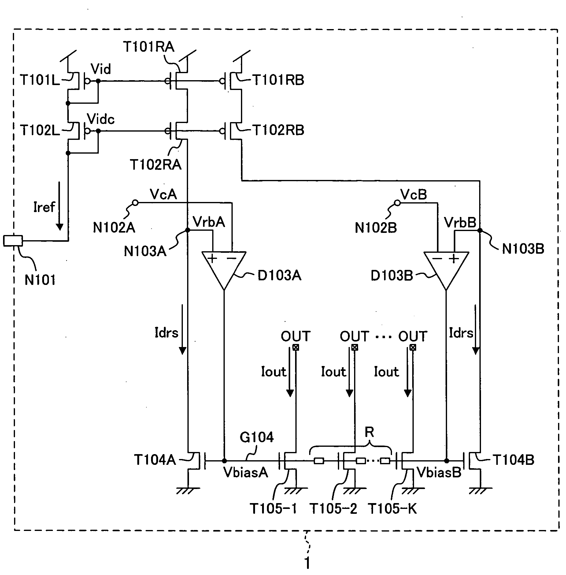
[0081]FIG. 1 shows the general structure of a current driver 1 according to embodiment 1 of the present invention. The current driver 1 includes a setting reference transistor T101L, supply reference transistors T101RA and T101RB, transistors T102L, T102RA and T102RB for cascode connection (hereinafter, “cascode connection transistor(s)”), reference current supply nodes N102A and N102B, differential amplifier circuits D103A and D103B, bias voltage generating transistors T104A and T104B, and K driving transistors T105-1 to T105-K (K is a natural number). The current driver 1 receives reference current Iref at a reference current input node N101. The current driver 1 is capable of allowing drain current Idrs, which has a current value equal or proportional to the current value of input reference current Iref, to flow through the bias voltage generating transistors T104A and T104B. The current driver 1 outputs output current lout, which has a current value equal or proportional t...

embodiment 2

[0139]

[0140] A plurality of transistors formed on one chip can have linearly-changing threshold voltage values. Alternatively, among a plurality of aligned transistors, the transistors provided at the central region have threshold voltage values smaller than those of the transistors at the both ends. In this case, the transistor characteristics of the transistors vary in an inverted “V” shape fashion.

[0141]

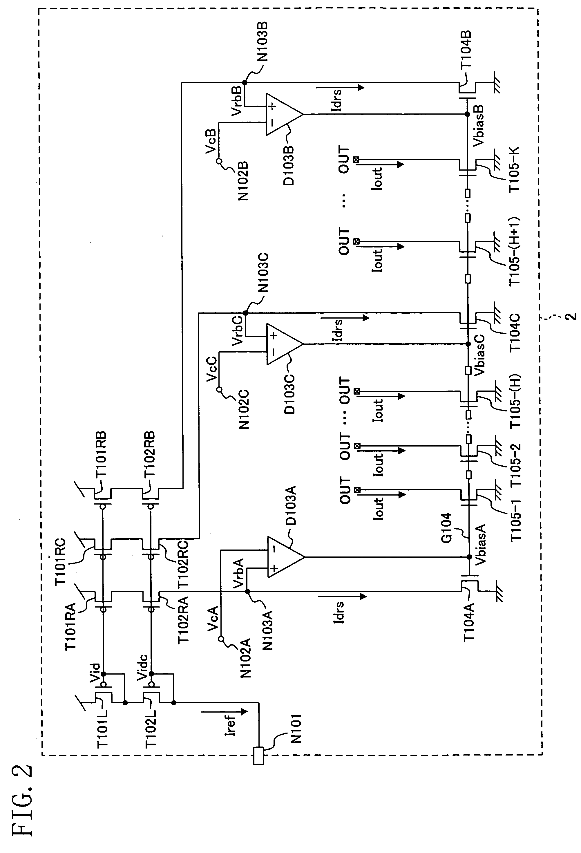
[0142]FIG. 1 shows the general structure of a current driver 2 according to embodiment 2 of the present invention. The current driver 2 includes, in addition to the components of the current driver 1 shown in FIG. 1, a supply reference transistor T101RC, a cascode connection transistor T102RC, a reference voltage supply node N103C, a differential amplifier circuit D103C, and a bias voltage generating transistor T104C. That is, the current driver 2 includes another set of a supply reference transistor, a cascode connection transistor, a reference voltage supply node, a differentia...

embodiment 3

[0164]

[0165]FIG. 3 shows the general structure of a current driver 3 according to embodiment 3 of the present invention. The current driver 3 includes, in addition to the components of the current driver 1 shown in FIG. 1, cascode transistors T301CA, T302CA, T303CA and T304CA, voltage limiting transistors T103A and T103B, and K output voltage limiting transistors T305-1 to T305-K.

[0166] The cascode transistors T301CA to T304CA are connected in series between the power supply node and the ground node. The cascode transistor T301CA is connected between the power supply node and the cascode transistor T302CA and has: a gate connected to the gate of the setting reference transistor T101L. The cascode transistor T302CA is connected between the cascode transistor T301CA and the cascode transistor T303CA and has a gate connected to the gate of the cascode connection transistor T102L. The cascode transistor T303CA is connected between the cascode transistor T302CA and the cascode transisto...


PUM


Abstract

In a current driver, a gate of a first generating transistor, gates of K driving transistors, and a gate of a second generating transistor are connected to a gate line in this order. A first differential amplifier outputs a voltage determined according to the difference between a voltage from a first supply node and a voltage at the drain of the first generating transistor. A second differential amplifier outputs a voltage determined according to the difference between a voltage from a second supply node and a voltage at the drain of the second generating transistor. The gate of the first generating transistor receives the output of the first differential amplifier. The gate of the second generating transistor receives the output of the second differential amplifier.

Description

CROSS-REFERENCE TO RELATED APPLICATION [0001] This application claims priority under 35 U.S.C. § 119(a) on Japanese Patent Application No. 2004-368740 filed on Dec. 21, 2004, the entire contents of which are hereby incorporated by reference. BACKGROUND OF THE INVENTION [0002] 1. Field of the Invention [0003] The present invention relates to a current driver and specifically to a current driver used as a display driver for an organic EL (Electro Luminescence) panel, or the like. [0004] 2. Description of the Prior Art [0005]<Structure of Conventional Current Driver>[0006]FIG. 11 shows a general structure of a conventional current driver 20. The conventional current driver 20 is referenced to reference current Iref as an input from the outside (e.g., from a current supply). The conventional current driver 20 includes a setting reference transistor T201L, supply reference transistors T201RA and T201RB, transistors T202L, T202RA and T202RB for cascode connection (hereinafter, “casc...

Claims


Application Information

Patent Timeline
Patent Type & Authority Applications(United States)
IPC IPC(8): H03K19/0175H05B44/00
CPCG09G3/3283G09G2320/0233H03F3/345H03F3/45179H03F3/45475
Inventor OMORI, TETSUROKOJIMA, HIROSHIMIZUKI, MAKOTO
Owner COLLABO INNOVATIONS INC
Why Eureka
Try Eureka