Film adhesive and semiconductor package using the same
a technology of film adhesive and semiconductor package, which is applied in the direction of heat-activated film/foil adhesive, film/foil adhesive, transportation and packaging, etc., can solve the problems of poor covering ability, warping of film, and uneven surface of substrate, and achieve excellent low-temperature adhesive properties. , the effect of simplifying the process
- Summary
- Abstract
- Description
- Claims
- Application Information
AI Technical Summary
Benefits of technology
Problems solved by technology
Method used
Image
Examples
synthesis example 1
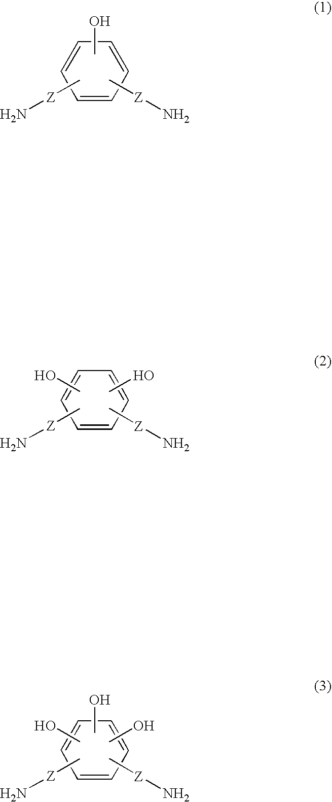
[0084] A 300-ml, 5-necked separable flask was provided with a stirrer, a nitrogen gas inlet tube, a thermometer and a Dienstag tube filled with mesitylene. 18.75 g of polytetramethyleneoxide-di-p-aminobenzoate (product name: ELASMER-1000, average molecular weight: 1,268, manufactured by Ihara Chemical Industry Co., Ltd.), 45.87 g of oxy-4,4′-diphthalic dianhydride, 100 g of N-methyl-2-pyrrolidone and 45 g of mesitylene were measured with the flask. The resulting mixture was dissolved in a nitrogen atmosphere. Thereinto was added 32.00 g of bisaminopropyltetramethyldisiloxane (product name: PAM-E, manufactured by Shin-Etsu Chemical Co., Ltd.) little by little. Then, the nitrogen gas inlet tube was inserted into the solution (in a bubbling state), and the solution was heated at a temperature of from 170° C. to 180° C. in the system with azeotropic removal of water and maintained for 12 hours. After cooling, 145 g of mesitylene was added for diluting and 0.93 g 4,4′-diamino-3,3′-dihydr...
synthesis example 2
[0086] A 300-ml, 5-necked separable flask was provided with a stirrer, a nitrogen gas inlet tube, a thermometer and a Dienstag tube filled with mesitylene. 15.00 g of 1,3-bis(3-(3-aminophenoxy)phenoxy)benzene, 43.44 g of silicone diamine (α,ω-bis(3-aminopropyl)polydimethylsiloxane (BY16-853U, average molecular weight: 920, manufactured by Dow Corning Toray Silicone Co., Ltd.), 110.61 g of N-methyl-2-pyrrolidone and 47.40 g of mesitylene were measured with the flask. The resulting mixture was heated at 50° C. in a nitrogen atmosphere for dissolving. Thereinto were added 18.49 g of oxy-4,4′-diphthalic dianhydride and 8.15 g of ethylene glycol bistrimellitic dianhydride little by little. Then, the nitrogen gas inlet tube was inserted into the solution (in a bubbling state), and the solution was heated at a temperature of from 170° C. to 180° C. in the system with azeotropic removal of water and maintained for 30 hours to avoid bumping. A solution of a thermoplastic polyimide was obtain...
synthesis example 3
[0088] A 500-ml, 5-necked separable flask was provided with a stirrer, a nitrogen gas inlet tube, a thermometer and a Dienstag tube filled with mesitylene. 13.95 g of polytetramethyleneoxide-di-p-aminobenzoate(product name: ELASMER-1000, manufactured by Ihara Chemical Co., Ltd.), 28.00 g of 1,3-bis(3-aminophenoxy)benzene, 34.12 g of oxy-4,4′-diphthalic dianhydride, 100 g of N-methyl-2-pyrrolidone and 40 g of mesitylene were measured with the flask. The resulting mixture was dissolved in a nitrogen atmosphere. Then, the nitrogen gas inlet tube was inserted into the solution (in a bubbling state), and the solution was heated at a temperature of from 170° C. to 180° C. in the system with azeotropic removal of water and maintained for 12 hours. After cooling, 290 g of N-methyl-2-pyrrolidone was added for diluting and 0.70 g 4,4′-diamino-3,3′-dihydroxybiphenyl (product name: HAB, manufactured by Wakayama Seika Kogyo Co., Ltd.) were added to obtain a solution of a thermoplastic polyimide....
PUM
| Property | Measurement | Unit |
|---|---|---|
| Temperature | aaaaa | aaaaa |
| Temperature | aaaaa | aaaaa |
| Temperature | aaaaa | aaaaa |
Abstract
Description
Claims
Application Information
 - R&D
- Intellectual Property
- Life Sciences
- Materials
- Tech Scout
- Unparalleled Data Quality
- Higher Quality Content
- 60% Fewer Hallucinations
Browse by: Latest US Patents, China's latest patents, Technical Efficacy Thesaurus, Application Domain, Technology Topic, Popular Technical Reports.
© 2025 PatSnap. All rights reserved.Legal|Privacy policy|Modern Slavery Act Transparency Statement|Sitemap|About US| Contact US: help@patsnap.com

