
Sram ring oscillator

a ring oscillator and sram technology, applied in the field of circuit typology, can solve the problems of inability to accurately predict ac read/write operations in sram memory arrays, inability to use fet models that are used to model hardware, and inability to accurately predict ac read/write operations in fet models. achieve the effect of accurate model to hardware correlation and easy construction

Active Publication Date: 2006-05-11
GLOBALFOUNDRIES US INC
View PDF8 Cites 31 Cited by
  • Summary
  • Abstract
  • Description
  • Claims
  • Application Information

AI Technical Summary

Benefits of technology

[0005] Another object of the invention is the provision of small, easy to build, and high yield circuit that provides AC model characterization and accurate model to hardware correlation.
[0007] Briefly, this invention contemplates provision of an SRAM design evaluation circuit topology in which the gates of the SRAM cell pass Gate Field Effect Transistors (FETs) are connected to the cross-coupled gates of the inverter pair of the SRAM cell. This evaluation circuit typology is used in a full cell implementation. A series of full cells are interconnected one to another in a loop to form a ring oscillator. The output of the ring is frequency divided and measured to study the read and write behavior of the cell design. Similarly, the half-cells, with the gate of its pass gate grounded, are interconnected one to another to form another ring oscillator, the output of which is frequency divided and measured to help isolate pass gate impact on memory function. The modified SRAM cell topology connected as a ring oscillator in hardware can be used to fully characterize an SRAM cell design, without the use of peripheral read / write circuitry. It provides AC model characterization and accurate model to hardware correlation. It is a simple and small circuit, easy to build and with a high yield. Using it in a ring oscillator enables cycle time measurement, delay and switching characteristics for individual SRAM cells, and for isolation of pass gate and in-board devices and for analysis of each separately. Comparison of high VT and low VT effects on cell performance and performance comparisons among different cell layouts can also be made. In addition, it can be put on chip process / device monitoring structures for product SRAM cell monitoring and characterization.

Problems solved by technology

SRAM circuit designs are very hard to model accurately because of the small size of the SRAM cell.
FET models that are used to model hardware are limited in their application to SRAM cells as these models are based on DC type measurements.
These FET models are not accurate in predicting AC Read / Write operations in SRAM memory arrays.
SRAM cells are sensitive devices whose performance is greatly affected by process imperfections and process variations.
Due to its small device widths, the SRAM is sensitive to process parameter variations, and in addition does not scale well with changes in technology.
Hence the characterization of the SRAM cell itself is often limited to the accuracy of the peripheral circuits.
The prior art does not directly measure SRAM cell AC characteristics from hardware.

Method used


Image

  • Sram ring oscillator
  • Sram ring oscillator
  • Sram ring oscillator

Examples


Embodiment Construction

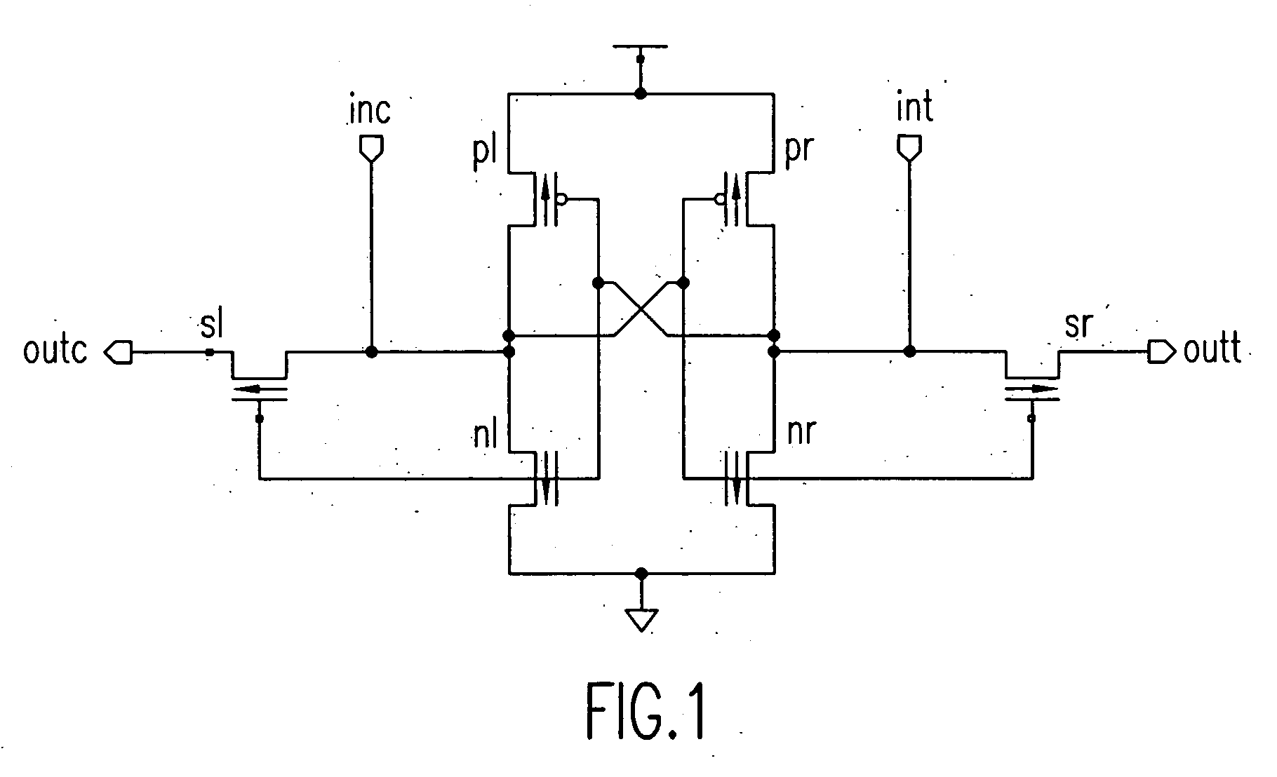
[0014] Referring now to FIG. 1 of the drawings, it shows a typical so called six transistors SRAM cell, modified in accordance with the teachings of this invention. It is comprised of complementary, cross-coupled, FET inverter pairs pl-nl, and pr-nr. But unlike a typical SRAM cell, the pass gates sl and sr of the cell are coupled to the gates of the corresponding cross-coupled inverter pairs, pl-nl and pr-nr, respectively. Coupled as a dual phase, ring oscillator, the two complementary inputs to each cell are int and inc, and the two complementary outputs are outc and outt.

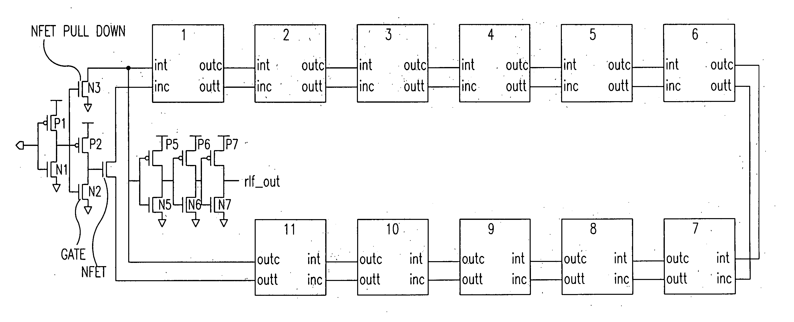
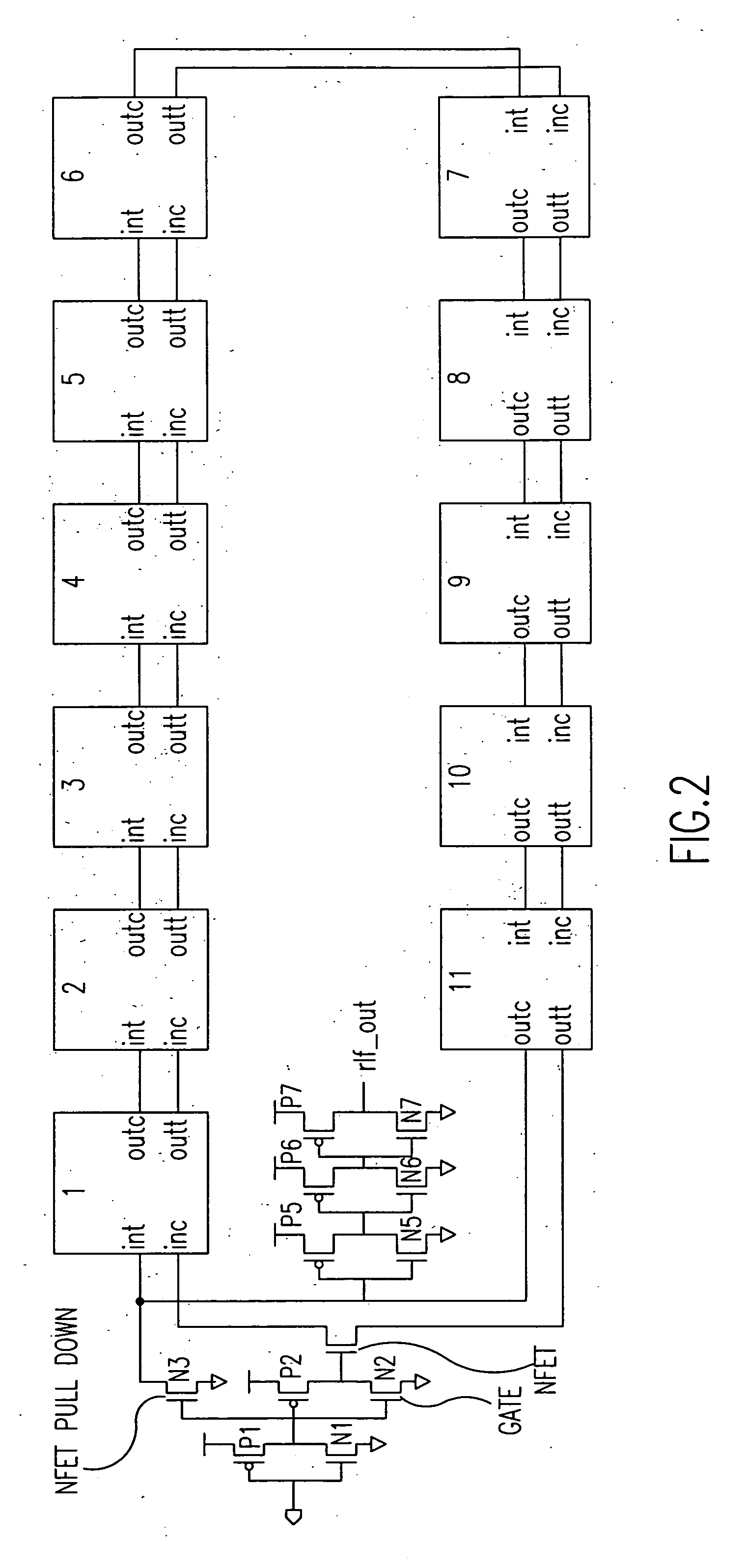
[0015]FIG. 2 shows a series eleven SRAM cells, each with the topology shown in FIG. 1, interconnected to form a dual phase ring oscillator. The outputs outc and outt of each cell in the series is coupled to the complementary inputs int and inc respectively of the next cell. That is, the output outt, shown in FIG. 1, of each cell in the series is connected to the input inc of the next cell and the output outc is c...


PUM


Abstract

An SRAM design evaluation circuit topology has the gates of the SRAM cell pass Gate Field Effect Transistors (FETs) connected to the cross-coupled gates of the inverter pair of the SRAM cell. This evaluation circuit typology is used in a full cell implementation. A series of full cells are interconnected one to another in a loop to form a ring oscillator. The output of the ring is frequency divided and measured to study the read and write behavior of the cell design. Similarly, half-cells, with the gates of their pass gates grounded, are interconnected one to another to form a ring oscillator, the output of which is frequency divided and measured to help isolate pass gate impact on memory function. The modified SRAM cell topology, connected as a ring oscillator in hardware, can be used to fully characterize an SRAM cell design, without the use of peripheral read / write circuitry.

Description

FIELD OF THE INVENTION [0001] This invention relates to a circuit typology for evaluating the design of a Static Random Access Memory (SRAM), and more particularly to a circuit typology that provides AC model characterization of the SRAM design with accurate model to product correlation. BACKGROUND [0002] SRAM circuit designs are very hard to model accurately because of the small size of the SRAM cell. SRAM performance data, based on traditional modeling and simulation often does not represent the performance of the hardware, it was intended to model and simulate. FET models that are used to model hardware are limited in their application to SRAM cells as these models are based on DC type measurements. These FET models are not accurate in predicting AC Read / Write operations in SRAM memory arrays. There are several reasons for this. SRAM cells are sensitive devices whose performance is greatly affected by process imperfections and process variations. An SRAM cell has unique propertie...

Claims


Application Information

Patent Timeline
IPC IPC(8): H03K3/03
CPCG01R31/31725G01R31/318364H03K3/0322
Inventor CHAN, YUEN H.SRINIVASAN, UMA
Owner GLOBALFOUNDRIES US INC
Learn More