
Method of address distribution time reduction for high speed memory macro

Inactive Publication Date: 2006-04-20
TOSHIBA AMERICA ELECTRONICS COMPONENTS +2
View PDF2 Cites 0 Cited by
  • Summary
  • Abstract
  • Description
  • Claims
  • Application Information

AI Technical Summary

Benefits of technology

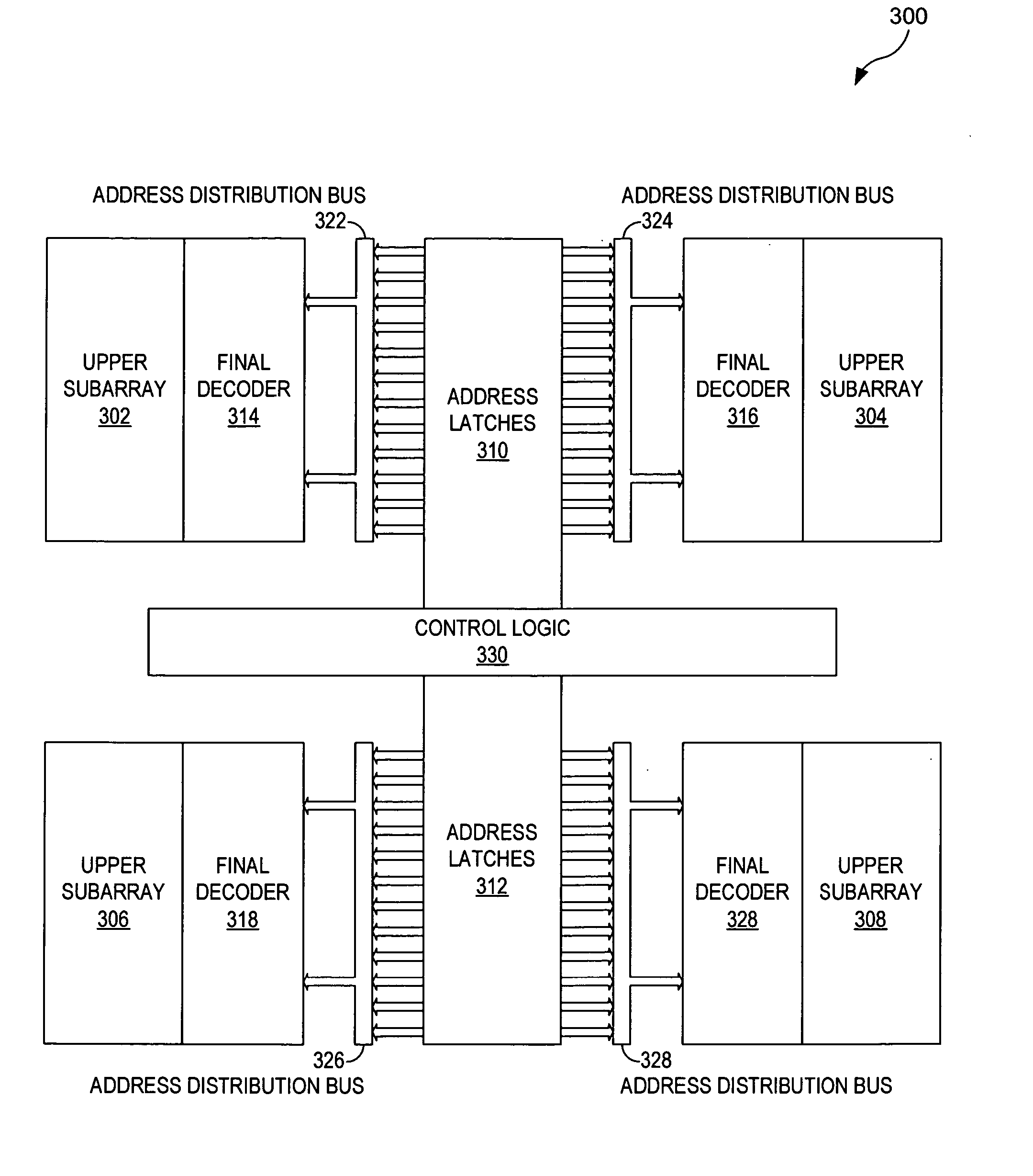
[0010] The present invention provides a method, an apparatus, and a computer program for the reduction of time delay and the conservation of energy during address signal distribution inside a high speed memory macro. The memory array in a conventional macro is divided into pairs of subarrays. Conventional memory address latches are also divided into separate sets of address latches. One set of memory address latches is interposed between each pair of subarrays. These address latches are configured to receive a global address signal and distribute that signal to the proper subarray. Before being stored in the proper subarray, the address signal is fully decoded by a final decoder. Further, a predecoder is combined with these sets of address latches to partially decode an address signal before it is distributed by the address latches. In addition, an enabling circuit is implemented to activate only the set of address latches that will be necessary for the specific address distribution. This design decreases time delay by shortening the wire length involved with address signal distribution and conserves energy by disabling one set of address latches during each address signal distribution.

Problems solved by technology

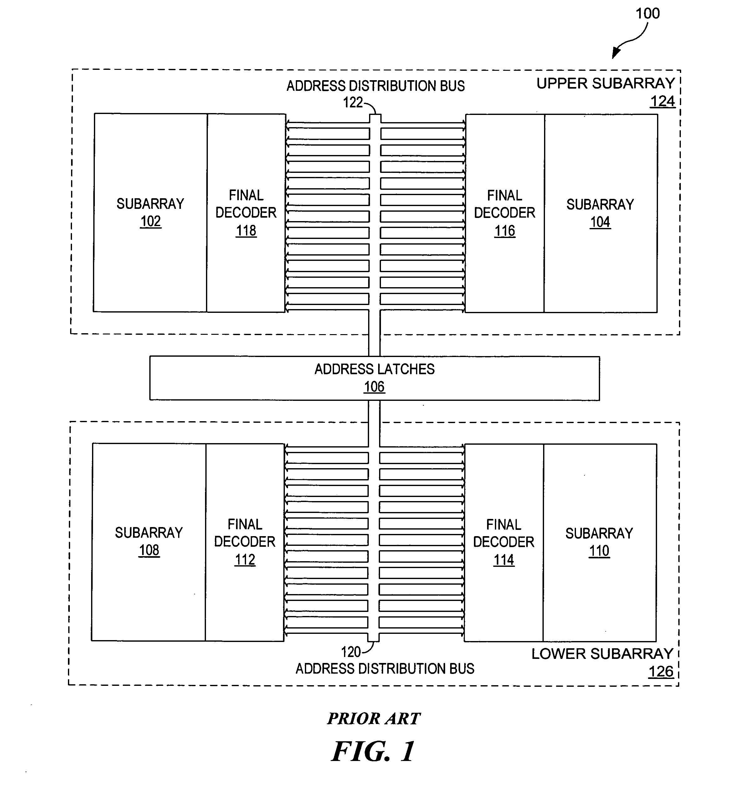
The problem with this design is that the address signals need to travel half of the length of a memory array height.
Any extra wire length will affect the distribution delay, skew, and slope of the signal.
One drawback of this design is that the address latches have to be powered on every time that a signal is destined for the upper subarray or the lower subarray.

Method used


Image

  • Method of address distribution time reduction for high speed memory macro
  • Method of address distribution time reduction for high speed memory macro
  • Method of address distribution time reduction for high speed memory macro

Examples


Embodiment Construction

[0018] In the following discussion, numerous specific details are set forth to provide a thorough understanding of the present invention. However, those skilled in the art will appreciate that the present invention may be practiced without such specific details. In other instances, well-known elements have been illustrated in schematic or block diagram form in order not to obscure the present invention in unnecessary detail. Additionally, for the most part, details concerning network communications, electromagnetic signaling techniques, and the like, have been omitted inasmuch as such details are not considered necessary to obtain a complete understanding of the present invention, and are considered to be within the understanding of persons of ordinary skill in the relevant art.

[0019] Referring to FIG. 3 of the drawings, the reference numeral 300 designates a modified high speed memory macro, wherein two sets of address latches 310 and 312 are placed in the center of the upper suba...


PUM


Abstract

An apparatus, a method, and a computer program product are provided for time reduction and energy conservation during address distribution in a high speed memory macro. To address these concerns, this design divides the typical data arrays into sets of paired subarrays, divides the conventional memory address latches into separate sets, and interposes one set of memory address latches between each pair of subarrays. Therefore, time is saved because the address signals have less wire length to travel and energy is saved because only one set of address latches needs to be powered on for each transmission.

Description

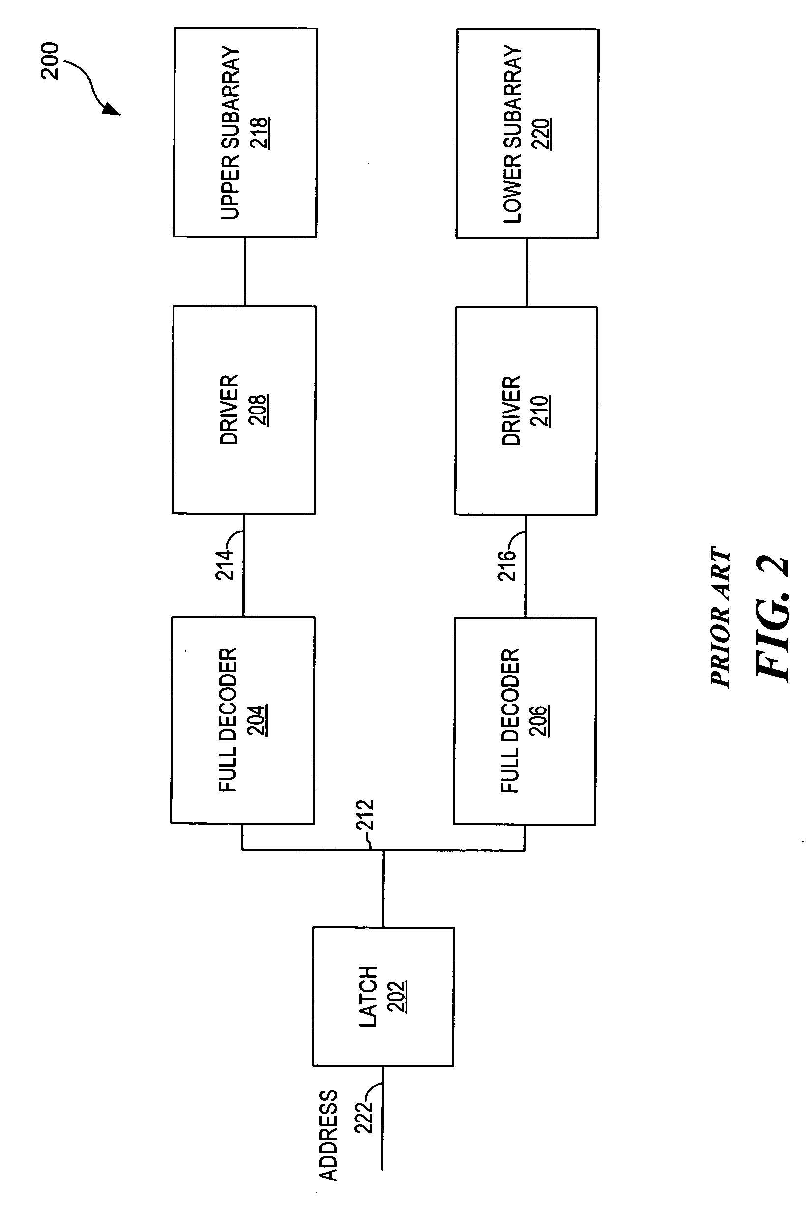
BACKGROUND OF THE INVENTION [0001] 1. Field of the Invention [0002] The present invention relates generally to address distribution in a high speed memory macro, and more particularly, to a method of time reduction and energy conservation during address distribution in a high speed memory macro. [0003] 2. Description of the Related Art [0004] High speed macros are used to realize high-performance operation of data processing systems and network designs. Specifically, high speed memory macros are used to distribute signals that can be stored as addresses. There is a constant search to decrease the time delay involved with distributing these address signals and to reduce the power involved with operating these macros. A high speed memory macro that distributes signals faster and with less power will be superior. [0005] Traditionally, in memory design one set of address latches is used to store information inside a high speed memory macro. The address latches are placed in the center o...

Claims


Application Information

Patent Timeline
IPC IPC(8): G11C8/00
CPCG11C8/06
Inventor DHONG, SANG HOOMURAKAMI, HIROAKIONISHI, SHOHJITAKAHASHI, OSAMU
Owner TOSHIBA AMERICA ELECTRONICS COMPONENTS
Learn More