Negative electrode for nonaqueous secondary battery
- Summary
- Abstract
- Description
- Claims
- Application Information
AI Technical Summary
Problems solved by technology
Method used
Image
Examples
examples
[0088] The present invention will now be illustrated in greater detail with reference to Examples, but it should be understood that the invention is not deemed to be limited thereto.
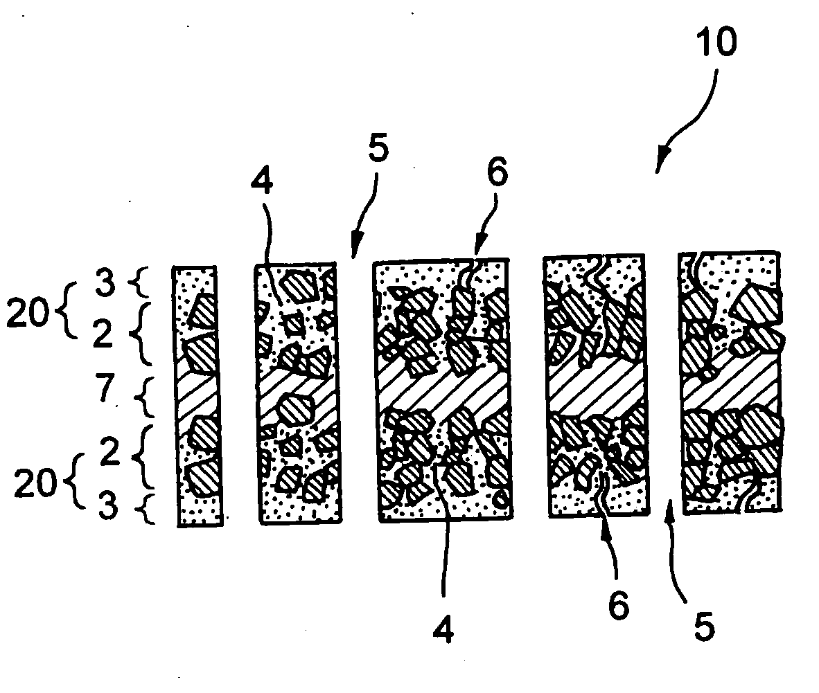
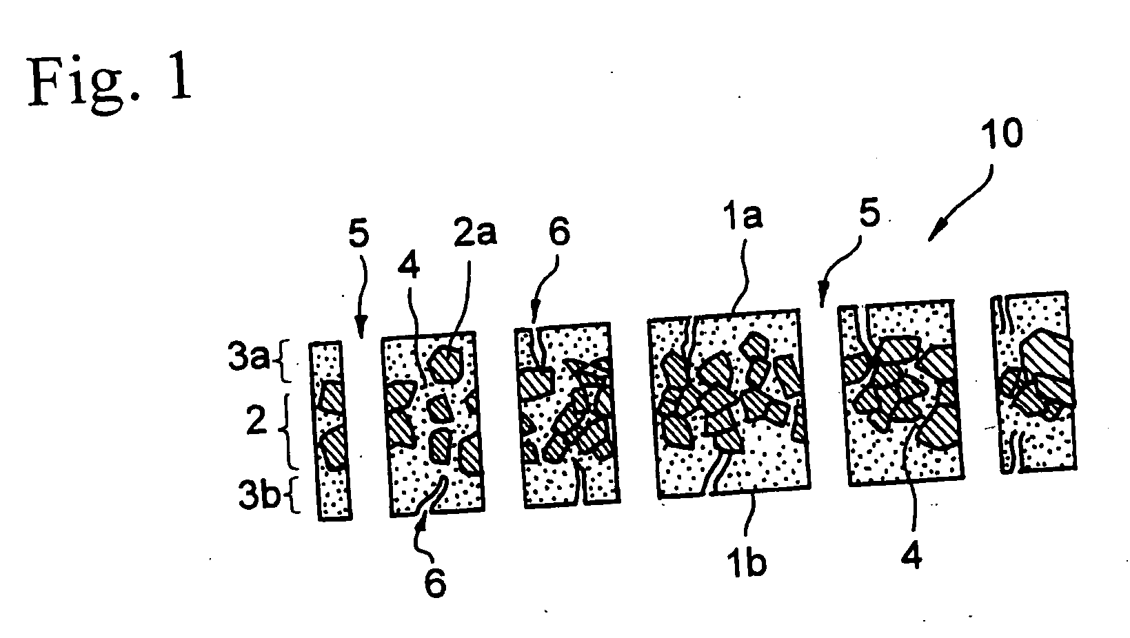
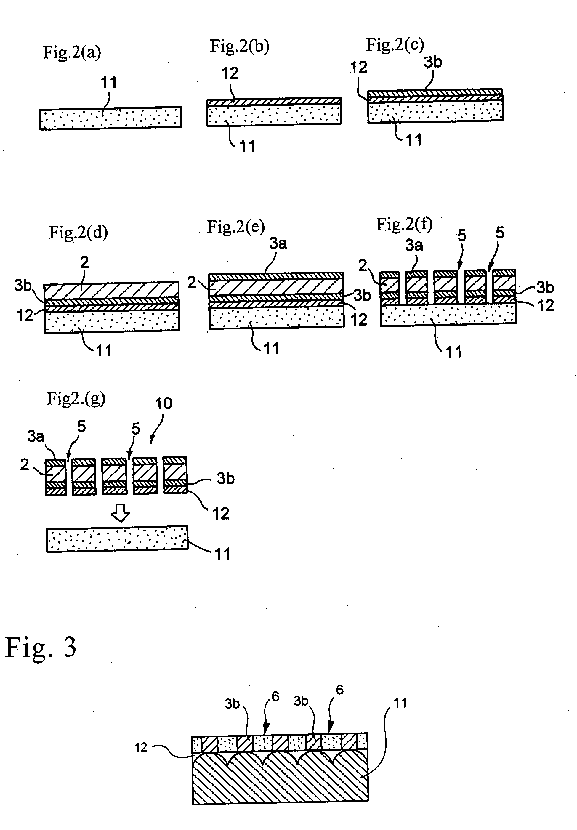
[0089] A negative electrode having the structure shown in FIG. 1, was prepared in accordance with the process illustrated in FIG. 2. A copper carrier foil (thickness: 35 μμm) obtained by electrolysis, was cleaned with an acid cleaning solution at room temperature for 30 seconds and then with pure water at room temperature for 30 seconds. The carrier foil was immersed in a 3.5 g / l CBTA solution kept at 40° C. for 30 seconds to form a release layer. After the treatment, the carrier foil was taken out of the solution and washed with pure water for 15 seconds.
[0090] A 2.5 wt % solution of polyvinylidene fluoride in N-methylpyrrolidone was applied to the rough side of the carrier foil (Ra=0.5 μm). The solvent vaporized to form a polymer film. The carrier foil coated with the polymer film was electroplated i...
example 2
[0097] A negative electrode shown in FIG. 4 was prepared in accordance with the process illustrated in FIG. 5. A 2.5 wt % solution of polyvinylidene fluoride in N-methylpyrrolidone was applied to the rough side of a carrier foil (Ra=0.5 μm). After the solvent vaporized to form a polymer film, the carrier foil was immersed in an H2SO4 / CuSO4-based plating bath containing 250 g / l of CuSO4 and 70 g / l of H2SO4 and electroplated at a current density of 5 A / dm2 to form a current collecting layer of copper having a thickness of 5 μm on the polymer film. The carrier foil taken out of the plating bath was washed with pure water for 30 seconds and dried in the atmosphere.
[0098] A slurry containing negative electrode active material particles was applied to the current collecting layer to a thickness of 15 μm to form an active material layer. The active material particles were silicon particles having a median diameter D50 of 2 μm. The slurry contained the active material, acetylene black, and...
example 3
[0103] A negative electrode shown in FIG. 6 was prepared. A negative electrode precursor supported on a carrier foil was made in the same manner as in Example 2. Separately, a 10 μm thick metallic lithium layer was formed on a side of a 5 μm thick copper foil (current collecting layer) by vacuum evaporation. The metallic lithium layer on the copper foil and the active material layer of the negative electrode precursor ,were brought into contact with each other to unite the copper foil and the negative electrode precursor.
[0104] A YAG laser beam was applied to the copper foil to regularly perforate 25 μm diameter holes going through the copper foil, the metallic lithium foil, and the negative electrode precursor at a pitch of 100 μm (10000 holes per square centimeter). Finally, the carrier foil was peeled off the current collecting layer to give a desired negative electrode. The amount of the metallic lithium in the negative electrode was 25% of the saturated reversible capacity of ...
PUM
| Property | Measurement | Unit |
|---|---|---|
| Fraction | aaaaa | aaaaa |
| Fraction | aaaaa | aaaaa |
| Thickness | aaaaa | aaaaa |
Abstract
Description
Claims
Application Information
 - R&D
- Intellectual Property
- Life Sciences
- Materials
- Tech Scout
- Unparalleled Data Quality
- Higher Quality Content
- 60% Fewer Hallucinations
Browse by: Latest US Patents, China's latest patents, Technical Efficacy Thesaurus, Application Domain, Technology Topic, Popular Technical Reports.
© 2025 PatSnap. All rights reserved.Legal|Privacy policy|Modern Slavery Act Transparency Statement|Sitemap|About US| Contact US: help@patsnap.com


