Switch linearized track and hold circuit for switch linearization

a linearization and hold circuit technology, applied in the field of analog to digital signal conversion, can solve the problems of signal dependent sampling time error, noise and non-linearity of all s/h and/or t/h circuits, and the effect of reducing the number of signals

Active Publication Date: 2006-03-09
RGT UNIV OF CALIFORNIA
View PDF6 Cites 16 Cited by
  • Summary
  • Abstract
  • Description
  • Claims
  • Application Information

AI Technical Summary

Problems solved by technology

All S/H and/or T/H circuits are limited in performance by standard non-ideal factors such as jitter, kT/C noise, sampling group delay and bandwidth, and capacitor non-linearity, etc.
This signal dependent sampling time error contributes both to noise and to non-linearity.
In a small signal case when both switches are turned off at about the same time, early and late sampling time errors tend to be somewhat cancelled due to the symmetry in the differential sampling.
However, the asymmetry in ...

Method used


Image

  • Switch linearized track and hold circuit for switch linearization
  • Switch linearized track and hold circuit for switch linearization
  • Switch linearized track and hold circuit for switch linearization

Examples


Embodiment Construction

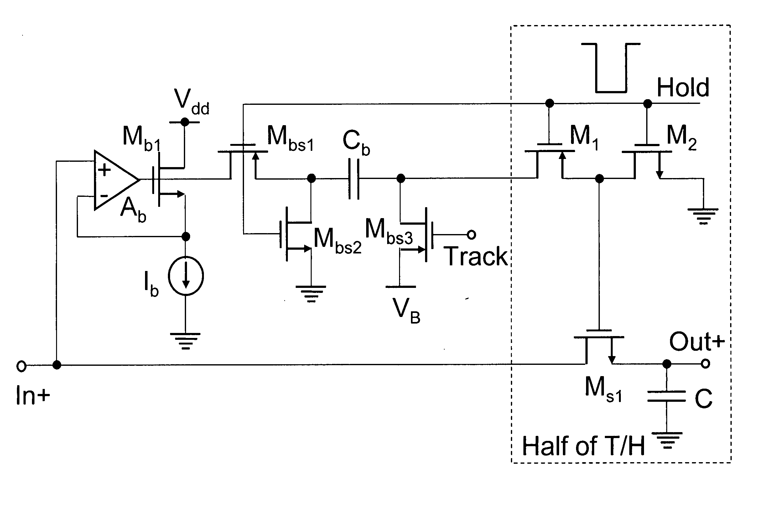
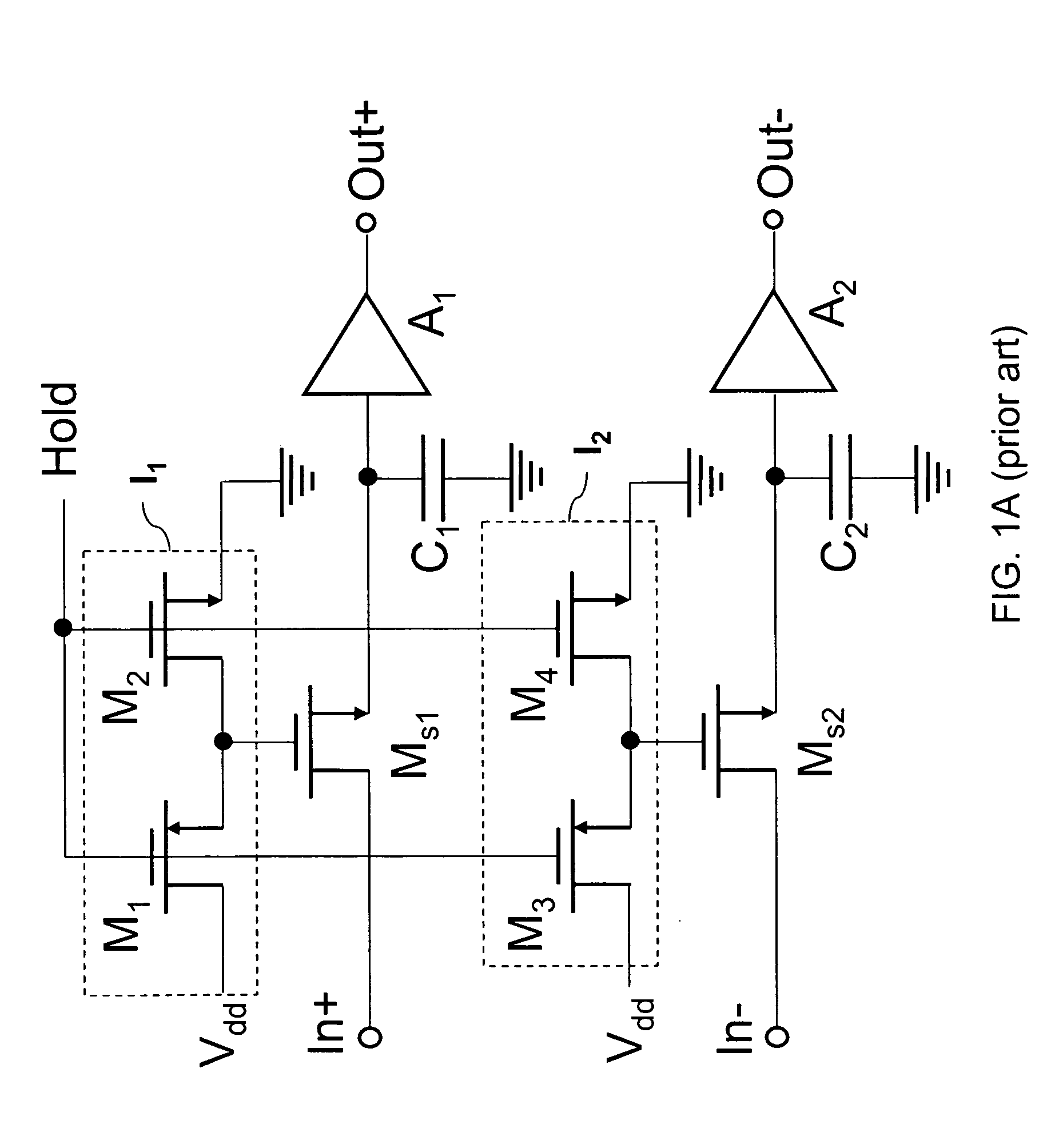
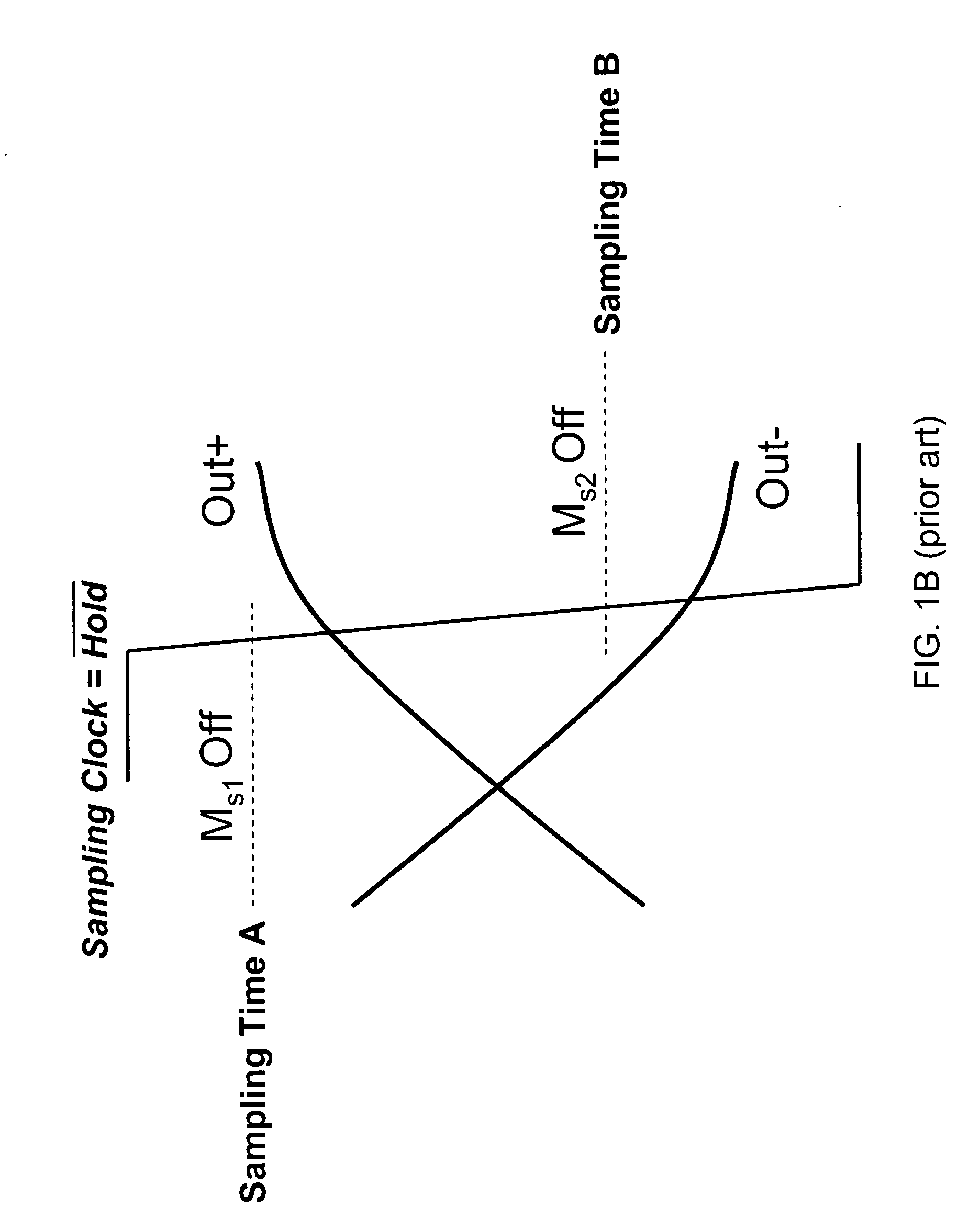
[0020] The sampling accuracy in CMOS T / H circuits is improved in embodiments of the invention by keeping switch on-resistance and channel charge injection constant. Embodiments of the invention provide CMOS T / H circuits that make the switch on-resistance and the channel charge injection linear and independent of the signal. Embodiments of the invention address problems with conventional circuits that have been identified by the present inventor. Unlike bottom-plate S / H circuits, conventional T / H circuits experience higher levels of error resulting from switch non-linearity, switch charge injection, and clock feed-through errors. In the differential T / H shown in FIG. 1A, the on-resistances of the two switches Ms1 and Ms2 vary as the input signal varies because the on-resistance is inversely proportional to the gate over-drive voltage over the threshold voltage. If this over-drive voltage is linearly proportional to the signal, the sum of the voltage drops across two switches Ms1 and ...


PUM


Abstract

Circuits that provide a gate boost to address non-linear threshold voltage variation in a CMOS T/H circuit. In embodiments of the invention, a boost capacitor and a feedback amplifier add a signal-dependent threshold voltage to the switch gate over-drive voltage of a switch that controls track and hold circuit sampling. In a modified embodiment, capacitive boost is omitted and the feedback amplifier provides the signal-dependent threshold voltage boost. In another embodiment, a boost capacitor and a diode connected transistor provide the signal-dependent threshold voltage boost. In a modified embodiment, capacitive boost is omitted and the diode connected transistor provides the signal-dependent threshold voltage.

Description

RELATED APPLICATION AND PRIORITY CLAIM [0001] This application is related to and claims priority under 35 U.S.C. § 119 from prior provisional application Ser. No. 60 / 608,508, filed Sep. 9, 2004.FIELD OF THE INVENTION [0002] The field of the invention is analog to digital signal conversion. An exemplary application of the invention is to CMOS track and hold circuits (T / H). BACKGROUND [0003] Sampled-data analog signal processing is widely used in analog / digital integrated systems. With an analog-to-digital converter (ADC) and proper sampling, most signal processing functions can be achieved digitally with high accuracy, which can meet or even exceed analog signal processing accuracy. Example signal processing functions used in a variety of applications from communications to measurement include filtering, timing recovery, and demodulation. [0004] During analog to digital conversion, the analog signal is sampled. This is typically achieved with sample-and-hold (S / H) or track-and-hold (...

Claims


Application Information

Patent Timeline
IPC IPC(8): G11C27/02
CPCG11C27/02H03K17/063G11C27/026G11C27/024
Inventor SONG, BANG-SUP
Owner RGT UNIV OF CALIFORNIA
Why Eureka
Try Eureka