
Electrostatic discharge (ESD) protection mos device and ESD circuitry thereof

a technology of electrostatic discharge and protection mos, which is applied in the direction of semiconductor devices, semiconductor/solid-state device details, electrical apparatus, etc., can solve the problems of destroying proper ic operation, physical destruction of circuit features, and significant problem of electrostatic discharge in integrated circuit design, so as to improve esd performance and robustness, improve esd performance, and occupies relatively small chip surface area

Active Publication Date: 2005-12-22
UNITED MICROELECTRONICS CORP
View PDF8 Cites 15 Cited by
  • Summary
  • Abstract
  • Description
  • Claims
  • Application Information

AI Technical Summary

Benefits of technology

The present invention provides an ESD protection device and ESD circuit that can protect against electrostatic discharge. The device includes an NMOS device with improved ESD performance and robustness. The NMOS device has an N type buried layer that borders the second ion well, fully isolating it from the silicon substrate. The device also includes a first isolation structure and a second isolation structure that are formed on the epitaxial silicon layer between the first and second ion wells. The NMOS device can be used in an integrated circuit chip to protect against electrostatic discharge. The technical effects of the invention are to provide a reliable and effective solution for protecting against electrostatic discharge in semiconductor devices.

Problems solved by technology

Electro-static discharge (ESD) is a significant problem in integrated circuit design, especially for devices with high pin counts and circuit speeds.
It is known that the inadvertent presence of a sudden voltage spike in an integrated circuit can cause physical destruction of circuit features.
For example, ESD-induced spikes can rupture the thin gate oxide of a field effect transistor (FET), or simply degrade the P-N junction of a semiconductor device, effectively destroying proper IC operation.
However, this approach requires additional circuitry.
As the sizes of the semiconductor MOS devices shrink to deep sub-micron scale, it becomes more difficult to control the “snapback” effect.
Accordingly, there remains an unsatisfied need for more sensitive and faster responding ESD circuits.

Method used


Image

  • Electrostatic discharge (ESD) protection mos device and ESD circuitry thereof
  • Electrostatic discharge (ESD) protection mos device and ESD circuitry thereof
  • Electrostatic discharge (ESD) protection mos device and ESD circuitry thereof

Examples


Embodiment Construction

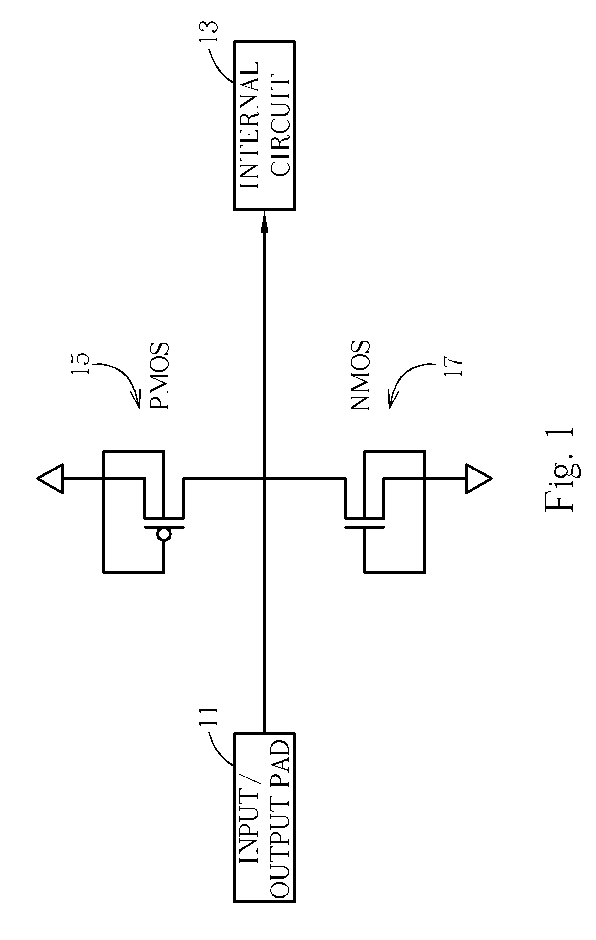
[0019]FIG. 1 shows a schematic diagram of an ESD protection circuit for IC input pads. The on-chip ESD protection circuit is built in IC chips to protect the devices and circuits against ESD damage. An input / output pad 11 is provided for interface with the internal circuit 13 of an IC chip. A PMOS 15 and an NMOS 17 are disposed between the input / output pad 11 and the internal circuit 13. According to one embodiment, the PMOS 15 and NMOS 17 devices are configured with their gates coupled to their respective sources. In general, for input pad protection, the junction breakdown voltages of the NMOS 17 and PMOS 15 should be smaller than the gate oxide breakdown voltage.

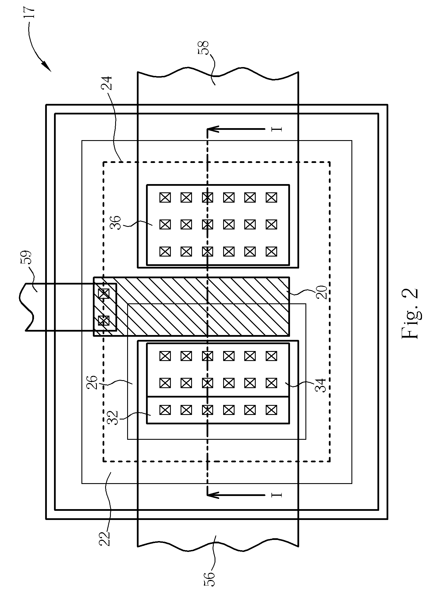
[0020] Referring to FIG. 2 and FIG. 3, wherein FIG. 2 is an enlarged plan view of the layout of the NMOS device 17 in accordance with the preferred embodiment of this invention; FIG. 3 is a schematic cross-sectional diagram showing the NMOS device 17 along line I-I of FIG. 2. According to the preferred embodiment of this...


PUM


Abstract

An NMOS device having protection against electrostatic discharge. The NMOS device includes a P-substrate, a P-epitaxial layer overlying the P-substrate, a P-well in the P-epitaxial layer, an N-well in the P-epitaxial layer and encompassing the P-well, an N-Buried Layer (NBL) underneath the P-well and bordering the N-well. The P-well is fully isolated by the N-well and the NBL. The NMOS device further includes a first isolation structure consisting of a gate-insulating layer connected with a field oxide layer, which is formed on the P-epitaxial layer. A gate overlies the first isolation structure. A second isolation structure laterally spaced apart from the first isolation structure is approximately situated on the N-well. An N+ source doping region, which functions as a source of the NMOS device, is disposed in the P-well. An N+ drain doping region, which functions as a drain of the NMOS device, is disposed in the N-well.

Description

CROSS-REFERENCES TO RELATED APPLICATIONS [0001] This is a continuation application of U.S. patent application Ser. No. 10 / 710,096, filed Jun. 18, 2004.BACKGROUND OF INVENTION [0002] 1. Field of the Invention [0003] The present invention relates to electrostatic discharge (ESD) protection of circuitry. More particularly, the present invention relates to ESD protection NMOS devices with enhanced triggering property and improved ESD robustness. According to one preferred embodiment of the present invention, an improved ESD protection NMOS device possessing a trigger voltage of about 43 volts and a second breakdown current (It2) of up to 2300 mA (measured by the transmission line pulse generator) is obtained. [0004] 2. Description of the Prior Art [0005] Electro-static discharge (ESD) is a significant problem in integrated circuit design, especially for devices with high pin counts and circuit speeds. ESD refers to the phenomena wherein a high-energy electrical discharge of current is p...

Claims


Application Information

Patent Timeline
Patent Type & Authority Applications(United States)
IPC IPC(8): H01L23/62H01L27/02H01L29/08H01L29/10H01L29/417H01L29/78
CPCH01L27/0266H01L29/0847H01L29/1083H01L29/861H01L29/41758H01L29/7801H01L29/41725H01L29/7816H01L29/0878
Inventor CHENG, CHIH-NANLU, YII-CHIANCHAO, FANG-MEI
Owner UNITED MICROELECTRONICS CORP
Learn More