Semiconductor device
a technology of a semiconductor and a capacitor, applied in the direction of semiconductor devices, electrical devices, transistors, etc., can solve the problems of reducing the resistance of the resistor, the inability to resist the feedback capacitance, and the oscillation phenomenon due to the feedback capacitance becoming an increasingly serious problem
- Summary
- Abstract
- Description
- Claims
- Application Information
AI Technical Summary
Benefits of technology
Problems solved by technology
Method used
Image
Examples
embodiment 1
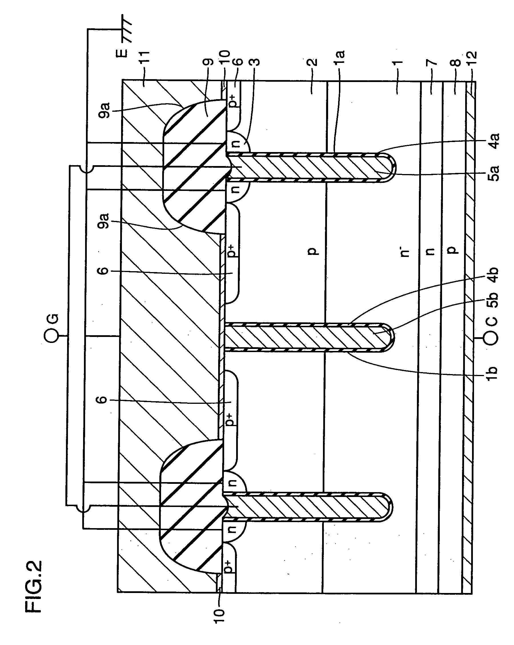
[0162]FIGS. 1 and 2 are a circuit diagram and a schematic cross sectional view showing the configuration of a semiconductor device according to Embodiment 1 of the present invention.
[0163] Referring primarily to FIG. 2, the semiconductor device of the present embodiment is a trench gate type IGBT formed in a semiconductor substrate having a thickness of, for example, 100 μm to 200 μm. An n− silicon substrate 1 has a concentration of, for example, approximately 1×1014 cm−3. A p-type body region 2 made of a p-type semiconductor, of which the concentration is, for example, approximately 1×1016 cm−3 to 1×1018 cm−3 and of which the depth from the first main surface is approximately 3 μm, is formed on the first main surface side of the above n− silicon substrate 1. An n-type emitter region 3 made of an n-type semiconductor, of which the concentration is, for example, 1×1019 cm−3, or higher, and of which the depth from the first main surface is approximately 0.5 μm, is formed in the first...
embodiment 2
[0201]FIG. 8 is a cross sectional view schematically showing the configuration of a semiconductor device according to Embodiment 2 of the present invention. In reference to FIG. 8, the semiconductor device of the present embodiment is a plane gate-type IGBT that is formed in a semiconductor substrate of which the thickness is, for example, approximately 100 μm to 200 μm. A p-type body region 2 made of a p-type semiconductor is selectively formed on the first main surface side of an n− silicon substrate 1 having a concentration of, for example, approximately 1×1014 cm−3. p-type body region 2 has a concentration of, for example, approximately 1×1016 cm−3 to 1×1018 cm−3 and has a depth of approximately 3 μm from the first main surface. An n-type emitter region 3 made of an n-type semiconductor having a concentration of, for example, 1×1019 cm−3, or greater, of which the depth from the first main surface is approximately 0.5 μm is formed in the first main surface within p-type body regi...
embodiment 3
[0212]FIG. 9 is a cross sectional view schematically showing the configuration of a semiconductor device according to Embodiment 3 of the present invention. In reference to FIG. 9, the configuration of the present embodiment differs from the configuration of Embodiment 1 in the relationship between trench 1a for a gate and the depth of trench 1b for an emitter. In the present embodiment, depth D2 where trench 1b for an emitter extends within the n− silicon substrate is set at a value greater than depth D1 where trench 1a for a gate extends within the n− silicon substrate. Thereby, a stabilizing plate capacitor Cf formed between stabilizing plate 5b and n silicon substrate 1 has a capacitance greater than that of a capacitor Cd on the gate side formed between gate electrode 5a and n silicon substrate 1.
[0213] Here, each depth D3 or D4 of trench 1a for gate or of trench 1b for an emitter from the first main surface is within a range of, for example, from 3 μm to 10 μm.
[0214] Here, t...
PUM
 Abstract
Description
Claims
Application Information
 - R&D
- Intellectual Property
- Life Sciences
- Materials
- Tech Scout
- Unparalleled Data Quality
- Higher Quality Content
- 60% Fewer Hallucinations
Browse by: Latest US Patents, China's latest patents, Technical Efficacy Thesaurus, Application Domain, Technology Topic, Popular Technical Reports.
© 2025 PatSnap. All rights reserved.Legal|Privacy policy|Modern Slavery Act Transparency Statement|Sitemap|About US| Contact US: help@patsnap.com


