Nanoscale arrays, robust nanostructures, and related devices
- Summary
- Abstract
- Description
- Claims
- Application Information
AI Technical Summary
Benefits of technology
Problems solved by technology
Method used
Image

Examples
example 1
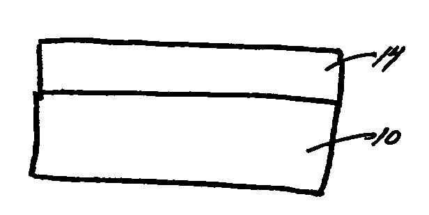
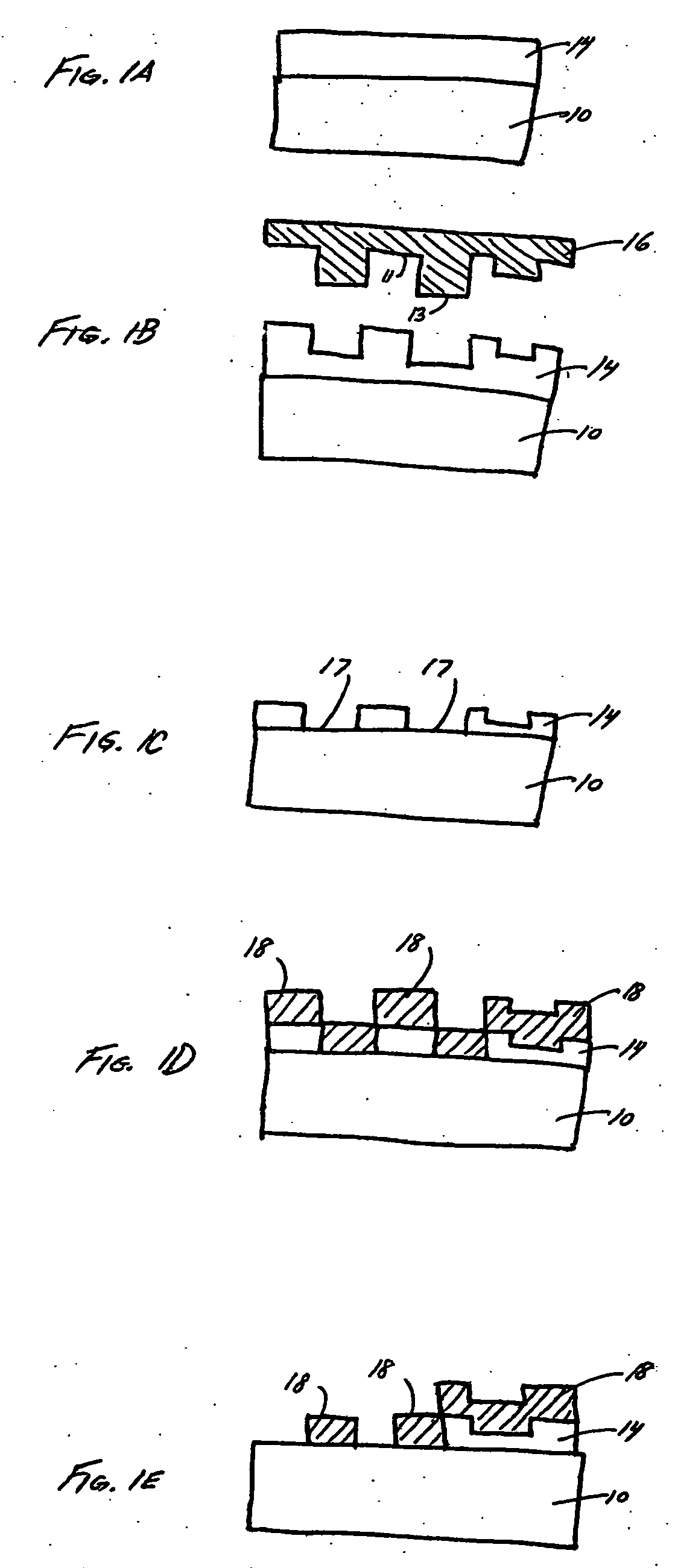
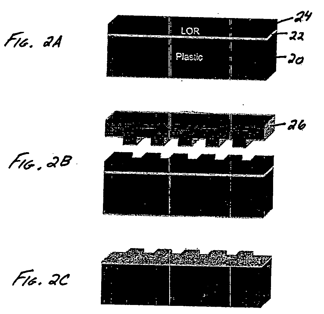
[0088] The merger of nanoscale devices with flexible plastics or polymers enables a broad spectrum of electronic and photonic applications. In this example, the use of room temperature nanoimprint lithography for the general fabrication of nanometer- through millimeter-scale patterns on polymer substrates is described. Specifically, the patterning of arrays of nanoscale source-drain electrode pairs with continuous interconnects to the millimeter length scale is shown, as well as the fabrication of hundred-nanometer gate features hierarchically patterned over large areas. These patterned polymeric substrates can also used in conjunction with semiconductor nanowires to assemble devices such as field-effect transistors.
[0089] In nanoimprint lithography (NIL), a relief pattern is generated via compression molding of an imprintable polymer by a stamp. This pattern is transferred to the underlying substrate by anisotropic reactive ion etching (RIE), followed by material deposition and li...
example 2
[0098] The merger of nanoscale building blocks with flexible and / or low cost substrates could enable the development of high-performance electronic and photonic devices with the potential to impact a broad spectrum of applications. This example demonstrates that high-quality, single-crystal nanowires can be assembled onto inexpensive glass and flexible plastic or polymer substrates to create basic transistor and light-emitting diode devices.
[0099] In this example, the high-temperature synthesis of single-crystal nanowires is separated from ambient-temperature solution-based assembly to enable the fabrication of single-crystal-like devices on virtually any substrate. To illustrate this, silicon nanowire field-effect transistors were assembled on glass and plastic substrates. These devices displayed device parameters rivaling those of single-crystal silicon and exceeding those of state-of-the-art amorphous silicon and organic transistors currently used for flexible electronics on pol...
example 3
[0110] This example illustrates nanowire transistor devices that were configured as low-threshold logic elements with gain; the high-performance characteristics were relatively unaffected by operation in a bent configuration or by repeated bending. In this example, a nanowire / plastic device similar to that described above with reference to the inset in FIG. 7A was used. The p-SiNWs used in this example to form p-n LEDs were core / shell structures 18 consisting of a 20-nm-diameter intrinsic silicon core and a 10-nm shell (250:1 Si / B).
[0111] The devices were fabricated on alkali-free glass wafers and 100-micron-thick poly(ethylene terephthalate) coated with approximately 100-nm-thick indium tin oxide, using techniques similar to those described in Example 2. The electrodes were defined by electron beam lithography and were metallized with Ti / Au (60 / 60 nm).
[0112] A comparison of Isd versus Vg data recorded when the nanowire / plastic device was flat versus bent to a radius of curvature ...
PUM
| Property | Measurement | Unit |
|---|---|---|
| Width | aaaaa | aaaaa |
| Flexibility | aaaaa | aaaaa |
| Transparency | aaaaa | aaaaa |
Abstract
Description
Claims
Application Information
 - R&D
- Intellectual Property
- Life Sciences
- Materials
- Tech Scout
- Unparalleled Data Quality
- Higher Quality Content
- 60% Fewer Hallucinations
Browse by: Latest US Patents, China's latest patents, Technical Efficacy Thesaurus, Application Domain, Technology Topic, Popular Technical Reports.
© 2025 PatSnap. All rights reserved.Legal|Privacy policy|Modern Slavery Act Transparency Statement|Sitemap|About US| Contact US: help@patsnap.com