Siloxane epoxy polymers as metal diffusion barriers to reduce electromigration
- Summary
- Abstract
- Description
- Claims
- Application Information
AI Technical Summary
Benefits of technology
Problems solved by technology
Method used
Image
Examples
example 1
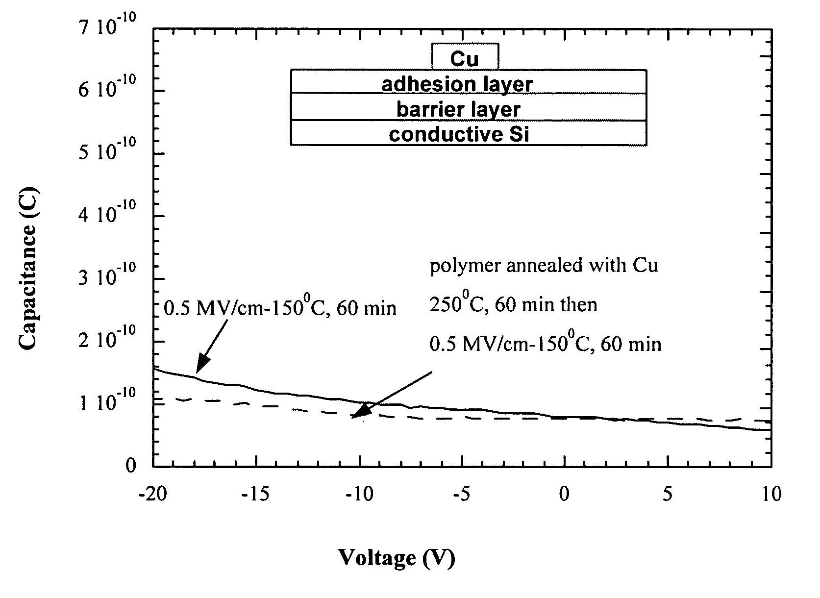
[0049] N-type, 4-inch silicon wafers having a resistivity of 0-0.02 ohm-cm for MIM (metal-insulator-metal) structures were used as the substrates. After standard RCA cleaning an adhesion layer (HMDS) was spin-coated onto each wafer at 3000 rpm for 40 sec. The wafers were then annealed in air at 100° C. for 10 min. A siloxane epoxy polymer solution containing formula (IIB), wherein the ratio of p to q was about 2:1, was spin-coated onto each wafer at 3000 rpm for 100 sec to a thickness of 0.5 μm. Onto the deposited polymer films, copper metal thin films were deposited to a thickness of 0.3 μm using sputtering or e-beam evaporation. The Cu / polymeric film / wafers were then dried under vacuum of 10−3 torr for 1 hour at 100° C. The samples were then cured at 165° C. for 2 hours to cross-link the polymer, followed by a thermal anneal at 250° C. under nitrogen gas flow for 1 hour. These films passed the industry-accepted Scotch® tape adhesion test, which was executed using commercially avai...
example 2
[0050] The procedure of Example 1 was followed. Then a thin layer of an adhesion promoter was deposited onto the copper surface of each sample. The adhesion promoter was also a siloxane epoxy polymer solution having formula (IIB), wherein the ratio of p to q was about 2:1, and was spin-coated onto the copper films at 3000 rpm for 100 sec to a thickness ranging from about 0.01 μm to about 0.03 μm. The samples were then dried under vacuum of 10−3 torr for 1 hour at 100° C., followed by curing at 165° C. for 2 hours and a thermal annea at 250° C. under nitrogen gas flow for 1 hour to cross-link the polymer. The surface of the polymeric adhesion promoter layer was then contacted with an aqueous solution of sulfuric acid (50% by weight) for 30 seconds at room temperature, followed by removal of the acid solution by rinsing with deionized water for 30 seconds at room temperature and drying. A second layer comprising a siloxane epoxy polymer solution containing formula (IIB), wherein the r...
example 3
[0051] N-type, 4-inch silicon wafers having a resistivity of 0-0.02 ohm-cm for MIM (metal-insulator-metal) structures were used as the substrates. After standard RCA cleaning, an adhesion layer (HMDS) was spin-coated onto each wafer at 3000 rpm for 40 sec. The wafers were then annealed in air at 100° C. for 10 min. A siloxane epoxy polymer solution, acting as a diffusion barrier and containing formula (IIB), wherein the ratio of p to q was about 2:1, was spin-coated onto each wafer at 3000 rpm for 100 sec to a thickness ranging from about 0.02 μm to about 0.05 μm. The polymeric film / wafers were dried under vacuum of 10−3 torr for 1 hour at 100° C. The polymer films were then cured at 165° C. for 2 hours to cross-link the polymer, followed by a thermal anneal at 250° C. under nitrogen gas flow for 1 hour. The surface of the polymeric diffusion barrier was then contacted with an aqueous solution of sulfuric acid (50% by weight) for 30 seconds at room temperature, followed by removal o...
PUM
 Abstract
Description
Claims
Application Information
 - R&D
- Intellectual Property
- Life Sciences
- Materials
- Tech Scout
- Unparalleled Data Quality
- Higher Quality Content
- 60% Fewer Hallucinations
Browse by: Latest US Patents, China's latest patents, Technical Efficacy Thesaurus, Application Domain, Technology Topic, Popular Technical Reports.
© 2025 PatSnap. All rights reserved.Legal|Privacy policy|Modern Slavery Act Transparency Statement|Sitemap|About US| Contact US: help@patsnap.com


