Semiconductor device having quantum well structure, and method of forming the same

a technology of semiconductor devices and well structures, which is applied in the direction of semiconductor devices, lasers, semiconductor lasers, etc., can solve the problems of difficult to form abrupt junctions in the quantum well structure, and difficult to form abrupt junctions between the ingan layers, so as to reduce stress and increase the number of interfaces

Inactive Publication Date: 2005-09-15
SUMITOMO ELECTRIC IND LTD
View PDF1 Cites 22 Cited by
  • Summary
  • Abstract
  • Description
  • Claims
  • Application Information

AI Technical Summary

Benefits of technology

[0009] In the semiconductor light emitting device disclosed in Document 2, the semiconductor layer referred to as the buffer layers is grown so as not to work as a substantial barrier layer. Since the lattice constant of the buffer layers is between that of the quantum well layers and that of the barrier layers, the buffer layers alleviate stress from the difference between the lattice constants of the barrier layer and the quantum well layer. But, a relatively large potential barrier is formed at respective interfaces in the following arrangements: between the quantum well layers and the buffer layers; between the buffer layers and the barrier layers. The quantum well structure increases the number of interfaces exhibiting the relatively large potential barrier because of the following: the lattice constant of the buffer layers is selected around the midpoint between that of the barrier layers and that of the well layer; the buffer layers and the well layer therebetween are inevitably located between the barrier layers.

Problems solved by technology

This decomposition makes it difficult to form abrupt junctions in the quantum well structure.
With increase of the number of growth of the InGaN layers, flatness of the surfaces of the InGaN layers is degraded growth by growth and thus it is difficult to form abrupt junctions between the InGaN layers.

Method used


Image

  • Semiconductor device having quantum well structure, and method of forming the same
  • Semiconductor device having quantum well structure, and method of forming the same
  • Semiconductor device having quantum well structure, and method of forming the same

Examples


first embodiment

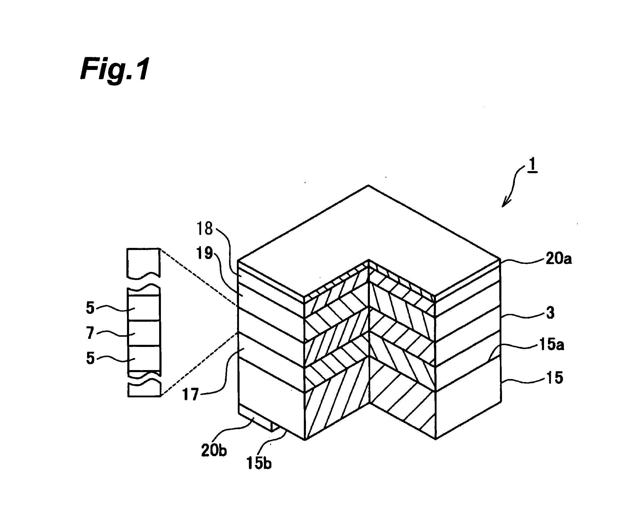
[0061]FIG. 1 is a view showing a semiconductor optical device. FIG. 2A to FIG. 2C are views showing some examples of the active region in semiconductor optical device. The semiconductor device 1 includes an active region 3 having a quantum well structure. The active region 3 includes well regions 5 and barrier region 7. The well regions 5 are made of a III-V nitride semiconductor containing nitrogen (N), indium (In) and gallium (Ga). The barrier region 7 is made of a III-V nitride semiconductor containing nitrogen (N), indium (In) and gallium (Ga).

[0062] As shown in FIG. 2A, a barrier region 7a has a first semiconductor layer 9a and a second semiconductor layer 11a. The first semiconductor layer 9a is made of a III-V compound semiconductor containing at least nitrogen (N), indium (In) and gallium (Ga) The second semiconductor layer 11a is made of a III-V compound semiconductor containing at least nitrogen (N) and gallium (N), and may contain indium (In). The first semiconductor lay...

second embodiment

[0091] A method of forming a semiconductor device having a quantum well structure will be described below. FIG. 7A and FIG. 7B are illustrations explaining a method of forming a semiconductor device as shown as the second embodiment of the present invention.

[0092] With reference to FIG. 7A, a substrate is prepared. The substrate can be, for example, a single-crystal wafer made of gallium nitride. A gallium nitride film may be grown on this wafer, if required. For example, organometallic vapor phase epitaxy (OMVPE) can be used to form this gallium nitride film and other III-V nitride semiconductor films formed in subsequent production steps. Subsequently, a method of forming a semiconductor device by use of gallium nitride substrate 21 will be described. A III-V nitride semiconductor film, such as a gallium nitride layer 23, is grown on the gallium nitride substrate 21. The gallium nitride film 23 has an n type conductivity. The gallium nitride film 23 can work as a cladding layer, ...

third embodiment

[0120] Next, a method of forming a semiconductor device having a quantum well structure will be described. FIG. 14A and FIG. 14B are illustrations explaining a method of forming a semiconductor device in the third embodiment of the present invention. This method is different in the following points from the embodiment shown in FIG. 9A and FIG. 9B: the temperature is increased in a period from time t7 to t9, the temperature is maintained at TB in a period M1 between time t9 and t21 (instead of time t10), and a barrier A film 30a is formed in a period from time t21 to t11. The temperature is increased in a period from time t16 to t18, the temperature is maintained at TB in a period M1 from time t18 to t22 (instead of time t19), and a barrier A film 34a is formed in a period between time t22 and t20.

[0121] In this example, the step of maintaining the temperature TB in the period M1 without forming a semiconductor film is provided after the previous barrier formation. In this period M1...


PUM

PropertyMeasurementUnit
thicknessaaaaaaaaaa
thicknessaaaaaaaaaa
temperatureaaaaaaaaaa

Abstract

A method of forming a semiconductor device having a quantum well structure, comprises the steps of: (a) forming a well film at a first temperature, the well film being made of a III-V nitride semiconductor containing nitrogen, indium and gallium; (b) forming a first barrier film on the well film, the first barrier film being made of a III-V nitride semiconductor containing nitrogen, indium and gallium, and an indium composition of the first barrier film being smaller than that of the well film; (c) changing temperature without forming a semiconductor film; and (d) forming a second barrier film at a second temperature higher than the first temperature, the second barrier film being made of a III-V nitride semiconductor on the first barrier film, the first barrier film being formed at a third temperature, the third temperature being equal to or higher than the first temperature, and the third temperature being lower than the second temperature.

Description

BACKGROUND OF THE INVENTION [0001] 1. Field of the Invention [0002] 2. Related Background Art [0003] The present invention relates to a semiconductor device having a quantum well structure and to a method of forming the same. BACKGROUND ART [0004] Document 1 (Japanese Patent Application Laid-Open No. 2001-168471) discloses a nitride semiconductor laser diode having a active layer with the quantum well structure. In the nitride semiconductor laser diode, the active layer has intermediate layers each of which is provided between one of well layers and one of barrier layers in the active layer. The intermediate layers are made of AldGa1-dN (0.30≦d≦1) and the bandgap energy of the intermediate layers is greater than that of the barrier layers. The addition of the intermediate layers can decrease the threshold voltage and driving voltage of the nitride semiconductor laser diode. This nitride semiconductor laser diode improves the luminous efficiency thereof by use of the AlGaN intermedia...

Claims


Application Information

Patent Timeline
Patent Type & Authority Applications(United States)
IPC IPC(8): H01L21/20H01L21/205H01L33/06H01L33/32H01S5/34H01S5/343
CPCB82Y20/00H01L33/06H01S5/34333H01S5/3407H01L33/32
Inventor KYONO, TAKASHIUENO, MASAKIAKITA, KATSUSHI
Owner SUMITOMO ELECTRIC IND LTD
Why Eureka
Try Eureka