
Circuit simulation system with simulation models assigned based on layout information and connection information

a circuit simulation and layout information technology, applied in computer aided design, analogue processes for specific applications, instruments, etc., can solve the problems of significant differences in characteristics between circuit elements classified in the same category, increase in parasitic resistance of source electrode region, and difference in the amount of voltage drop

Inactive Publication Date: 2005-09-08
KK TOSHIBA
View PDF5 Cites 18 Cited by
  • Summary
  • Abstract
  • Description
  • Claims
  • Application Information

AI Technical Summary

Problems solved by technology

However, there is a significant difference in characteristics between circuit elements classified in the same category due to the influence of adjacent circuit elements as a result of miniaturization of a semiconductor device.
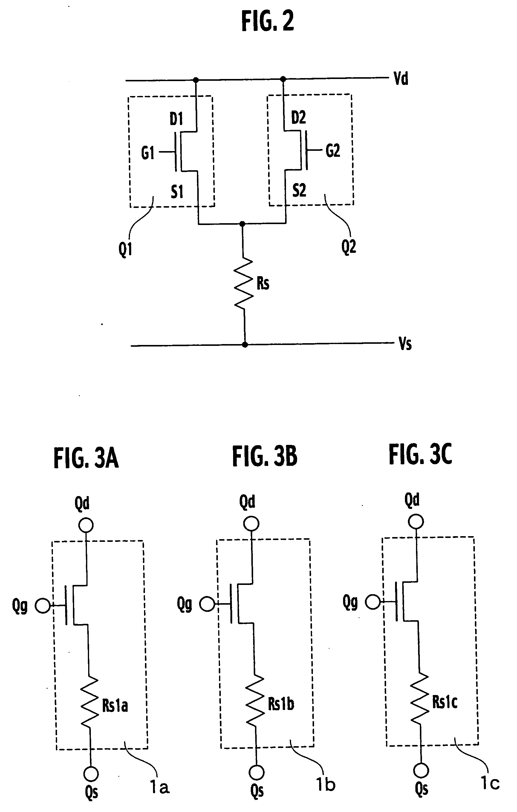
For example, the interface resistance of silicide formed on the source region of a MOS transistor increases as the semiconductor device is miniaturized, resulting in an increase in the parasitic resistance of the source electrode region.
This is because when current flows through two MOS transistors simultaneously, double current flows through the parasitic resistance of the common source electrode region, resulting in a difference in the amount of voltage drop.
Nevertheless, with method (i), the number of elements in the to-be-analyzed circuit increases, resulting in an increase in analysis time.
On the other hand, with method (ii), since circuit simulation assumes that all circuit states are executed, the circuit design has a large design margin, resulting in inhibition of a high-performance semiconductor device.
In addition, the characteristics of the circuit elements may differ due to temperature dependence on the circuit elements in the case of a large or a small power consumption emanating from circuit behavior of adjacent circuit blocks.
Furthermore, the characteristics of the adjacent circuit elements may differ due to the influence of the amount of noise generated in the circuit blocks.
Since not only circuit layout information but also circuit behavior information is needed to consider such influences upon the circuit elements from the circuit behavior of the adjacent circuit blocks, highly accurate circuit simulation cannot be executed by the Binning method.

Method used


Image

  • Circuit simulation system with simulation models assigned based on layout information and connection information
  • Circuit simulation system with simulation models assigned based on layout information and connection information
  • Circuit simulation system with simulation models assigned based on layout information and connection information

Examples


first embodiment

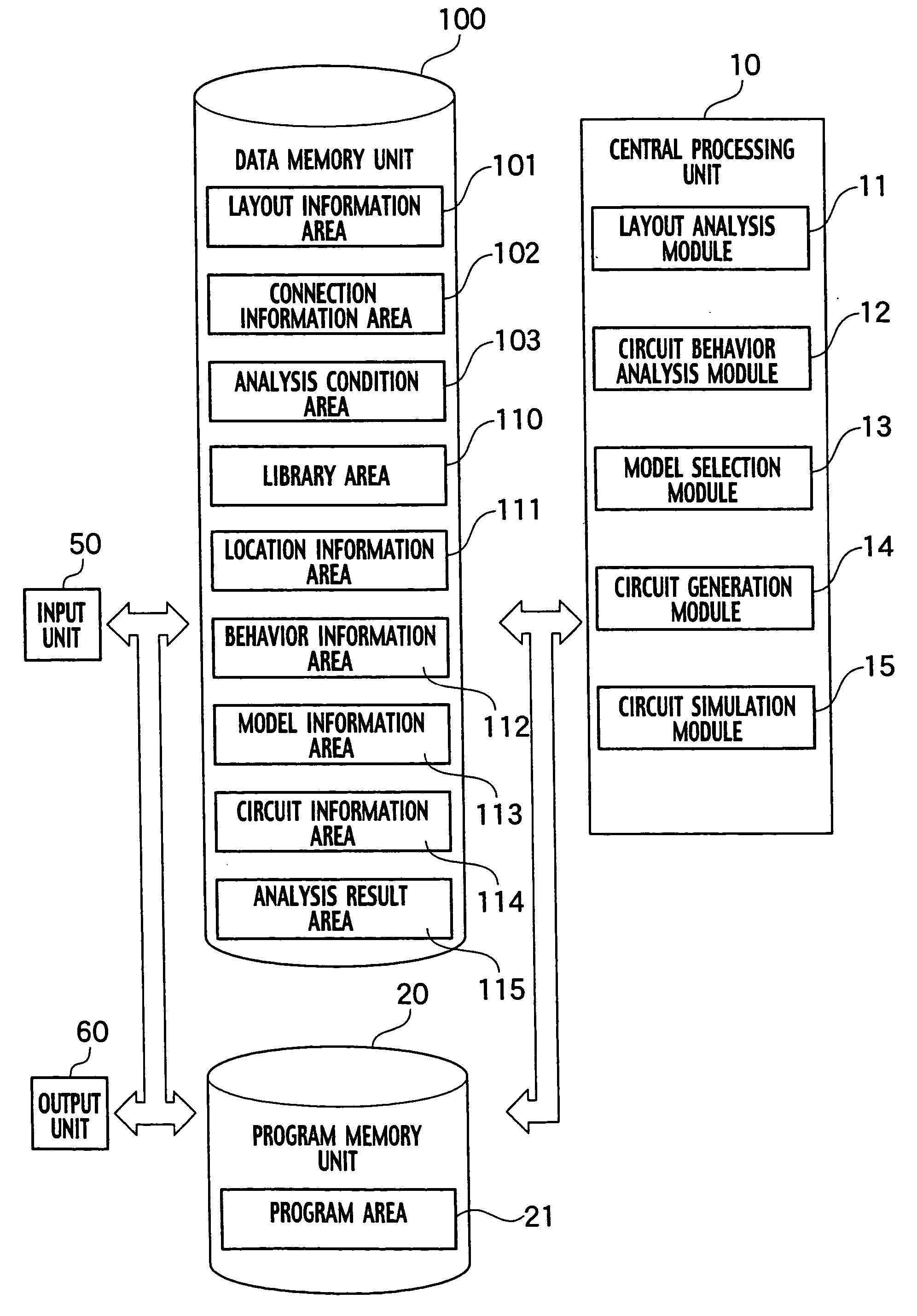
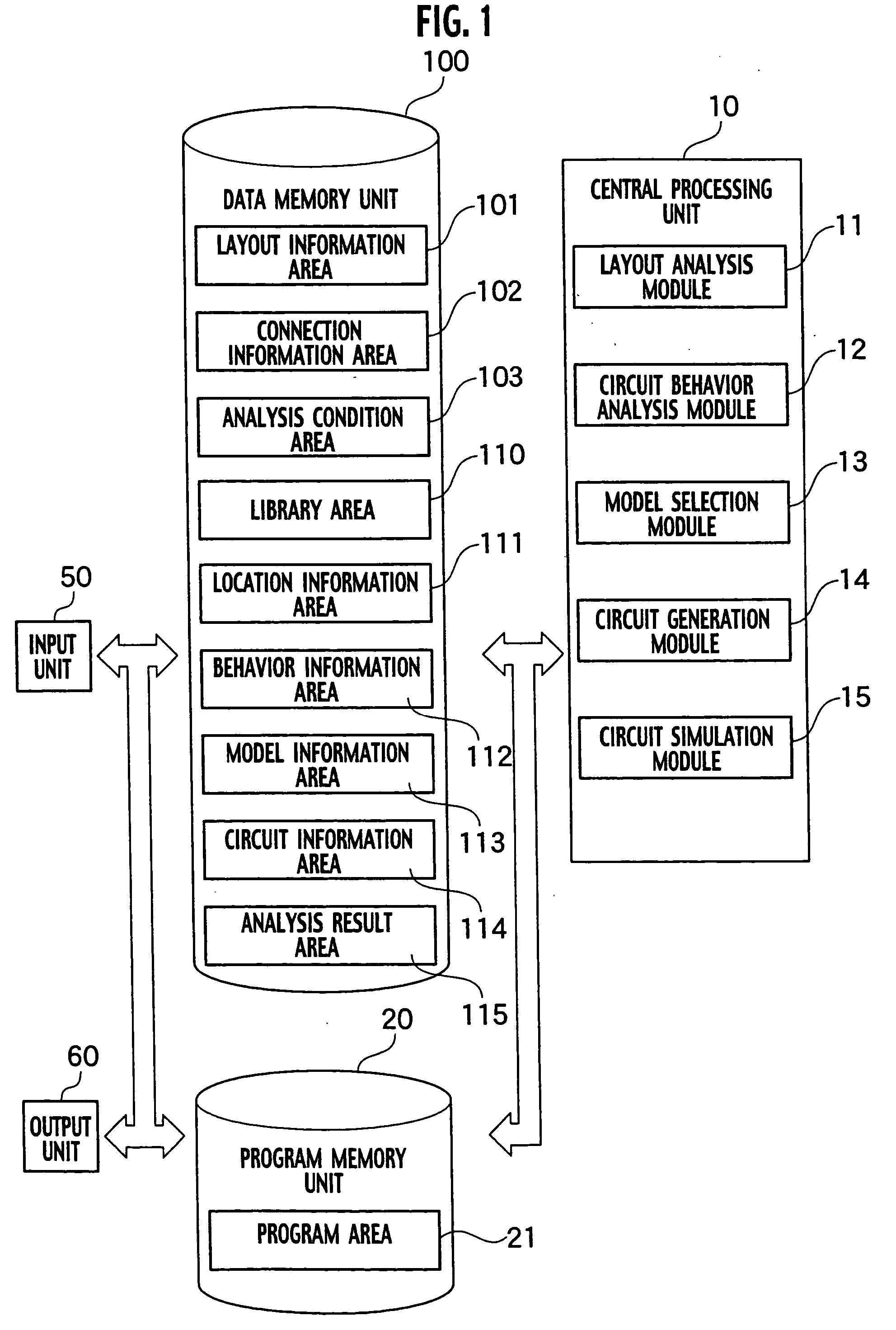
[0036] As shown in FIG. 1, a circuit simulation system according to the first embodiment of the present invention includes a CPU 10, a program memory unit 20, a data memory unit 100, an input unit 50, and an output unit 60.

[0037] The data memory unit 100 includes a layout information area 101, a connection information area 102, an analysis condition area 103, a library area 110, a location information area 111, a behavior information area 112, a model information area 113, a circuit information area 114, and an analysis result area 115. The layout information area 101 stores layout information for circuit elements of integrated circuits to be subjected to circuit simulation. Layout information includes information such as coordinates of the active region and coordinates corresponding to the layouts of circuit elements. The connection information area 102 stores electrical connection information of an integrated circuit to be subjected to circuit simulation. The analysis condition a...

second embodiment

[0084] Characteristics of a circuit element such as a transistor may change due to temperature change emanating from power consumption of adjacent circuit blocks and the like. The power consumption of a circuit block is determined depending on the circuit behavior of the circuit block. More specifically, an amount of current flowing to each circuit element in the circuit block is determined by whether or not the circuit elements included in the circuit block are conducting, and power consumption of the circuit block can be calculated based on that amount of current. Whether or not the circuit elements are conducting can be determined by circuit behavior based on the circuit connection information. Accordingly, power consumption of the circuit block can be estimated from the electrical connection information of the circuit block. In addition, the amount of change in temperature of a circuit element due to power consumption of a circuit block depends on the distance from the circuit b...


PUM


Abstract

A circuit simulation system for simulating an integrated circuit includes a circuit behavior analysis module analyzing behavior information of a circuit element of the integrated circuit based on connection information; a model selection module selecting a circuit element model corresponding to the circuit element from the library area based on location information and behavior information of the circuit element; a circuit generation module generating a to-be-analyzed circuit using the selected circuit element model; and a circuit simulation module executing the to-be-analyzed circuit simulation.

Description

CROSS REFERENCE TO RELATED APPLICATIONS [0001] This application is based upon and claims the benefit of priority from prior Japanese Patent Application P2004-060678 filed on Mar. 4, 2004; the entire contents of which are incorporated by reference herein. BACKGROUND OF THE INVENTION [0002] 1. Field of the Invention [0003] The present invention relates to a design method of an integrated circuit, particularly to a circuit simulation system, a circuit simulation method and a circuit simulation program. [0004] 2. Description of the Related Art [0005] In circuit simulation used for system circuit design, circuit elements such as transistors are classified according to characteristics thereof such as active region threshold voltage or polarity determined depending on the fabrication method. A unique circuit element model is provided for each category. However, there is a significant difference in characteristics between circuit elements classified in the same category due to the influence...

Claims


Application Information

Patent Timeline
IPC IPC(8): G06F17/50G06G7/62H01L21/82H01L21/822H01L27/04
CPCG06F17/5081G06F17/5036G06F30/367G06F30/398
Inventor INUKAI, TAKASHIURAKAWA, YUKIHIRO
Owner KK TOSHIBA
Learn More