Charged particle beam apparatus, charged particle detection method, and method of manufacturing semiconductor device

a technology of charged particle and beam apparatus, which is applied in the direction of semiconductor/solid-state device testing/measurement, instruments, and material analysis using wave/particle radiation. it can solve the problems of above-described detection methods, blurry focus, and difficulty in detecting them at a lower portion of the objective lens

Inactive Publication Date: 2005-06-30
KK TOSHIBA
View PDF4 Cites 19 Cited by
  • Summary
  • Abstract
  • Description
  • Claims
  • Application Information

AI Technical Summary

Problems solved by technology

In the scanning electron microscope disclosed in Japanese Patent Laid-Open No. 11-162384, the secondary electrons emitted from the wafer are accelerated between the wafer and the objective lens immediately after emission by an electrical field that draws them out on the electron gun side, in a state in which a negative potential (a retarding potential) is applied to the wafer, making it difficult to detect them at a lower portion of the objective lens.
However, the above-described detection methods have problems, as discussed below.
Specifically, the effect of the method disclosed in Japanese Patent Laid-Open No. 63-175325 only occurs with an optical system in which the distance from the objective lens to the wafer is sufficiently long and the negative potential applied to the metal casing is comparatively large (−50 to −150 V), which lead to blurriness of the focus.
In this low-acceleration voltage type of charged particle beam lithography apparatus, loss of focus of the beam due to the space charge effect becomes a problem, and thus it is essential to reduce the dimensions of the optical system in order to reduce this loss of focus.
For that reason, these methods cannot be applied to a low-acceleration voltage type of charged particle beam lithography apparatus in which the optical system must be compact.

Method used


Image

  • Charged particle beam apparatus, charged particle detection method, and method of manufacturing semiconductor device
  • Charged particle beam apparatus, charged particle detection method, and method of manufacturing semiconductor device
  • Charged particle beam apparatus, charged particle detection method, and method of manufacturing semiconductor device

Examples


first embodiment

(1) First Embodiment

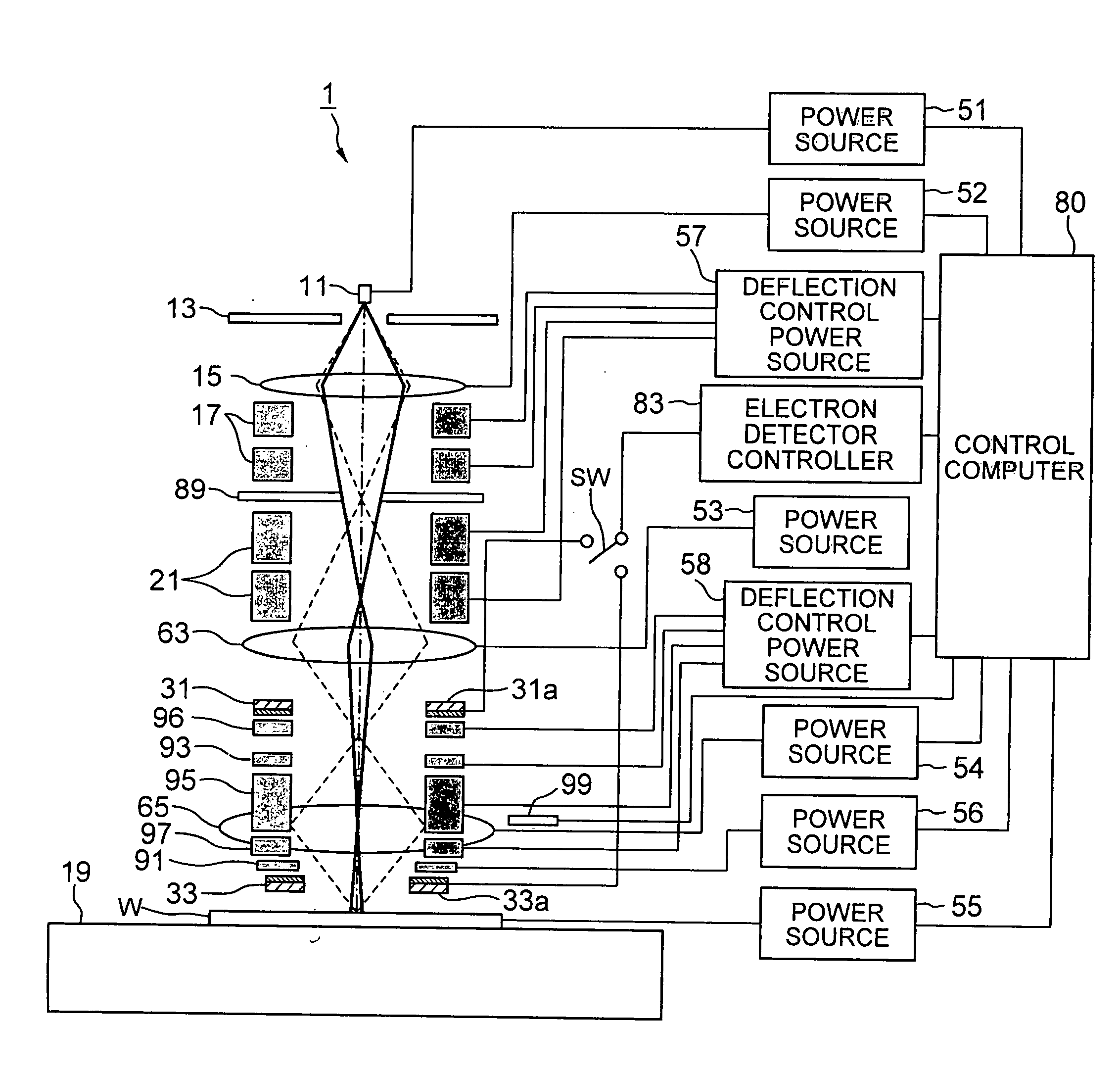
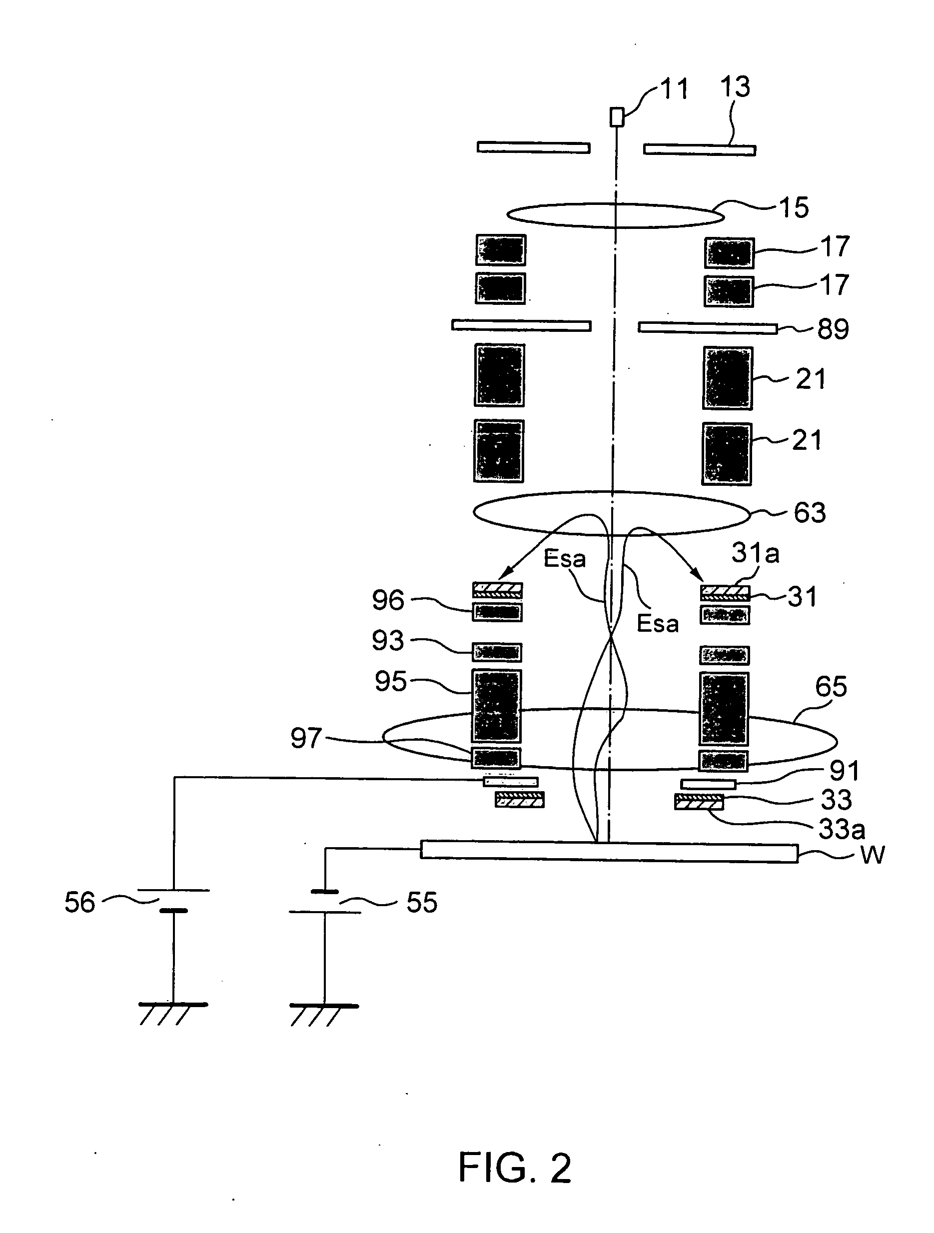
[0065] A block diagram of a first embodiment of the charged particle beam apparatus in accordance with the present invention is shown in FIG. 1A. An electron beam drawing system 1 shown in this figure comprises an electronic optical system, a controller, and an XY stage 19.

[0066] The controller includes a control computer 80 that controls the entire system, power sources 51 to 56, deflection control power sources 57 and 58, and an electron detector controller 83 that is specific to this embodiment. The electron detector controller 83 selectively receives signals representative to secondary electrons that have been detected by the secondary electron detectors 31 and 33 (as will be described later), by switching a switch SW, and transfer the signals to the control computer 80 as secondary electron signals that form SEM images. This point will be discussed later. The control computer 80 outputs SEM images by processing these secondary electron signals.

[0067] The X...


PUM

PropertyMeasurementUnit
incident velocityaaaaaaaaaa
inner diameteraaaaaaaaaa
voltageaaaaaaaaaa

Abstract

A charged particle beam apparatus includes: a charged particle beam source which generates a charged particle beam to irradiate the charged particle beam onto a specimen; a demagnification optical system which demagnifies the charged particle beam; a deflector which deflects the charged particle beam to scan the specimen; and a first charged particle detector having a detection surface to detect a charged particle generated from the specimen which has been irradiated with the charged particle beam; wherein the detection surface of the first charged particle detector is disposed so as to face towards the charged particle beam source.

Description

CROSS REFERENCE TO RELATED APPLICATION [0001] This application claims benefit of priority under 35USC §119 to Japanese Patent Application No. 2003-363242, filed on Oct. 23, 2003, the contents of which are incorporated by reference herein. BACKGROUND OF THE INVENTION [0002] 1. Field of the Invention [0003] The present invention relates to a charged particle beam apparatus, a charged particle detection method, and a method of manufacturing a semiconductor device. [0004] 2. Related Background Art [0005] Various methods have been proposed for increasing the efficiency of detection of secondary electrons generated from the surface of a specimen in a scanning electron microscope, such as a method of disposing a micro channel plate (MCP) detector and a metal casing to which a negative potential is applied, in a lower portion of the objective lens (such as that disclosed in Japanese Patent Laid-Open No. 63-175325) and a method of disposing an MCP detector in an upper portion of the objectiv...

Claims


Application Information

Patent Timeline
Patent Type & Authority Applications(United States)
IPC IPC(8): G01N23/225G21K5/04H01J37/08H01J37/20H01J37/244H01J37/305H01L21/027H01L21/66
CPCH01J37/244
Inventor NAGANO, OSAMUANDO, ATSUSHI
Owner KK TOSHIBA
Why Eureka
Try Eureka