Deflectable microstructure and method of manufacturing the same through bonding of wafers
- Summary
- Abstract
- Description
- Claims
- Application Information
AI Technical Summary
Benefits of technology
Problems solved by technology
Method used
Image
Examples
embodiment 3
[0076]FIG. 8 schematically shows a third preferred embodiment of the final mirror or mirror arrays device fabricated according to the invention.,
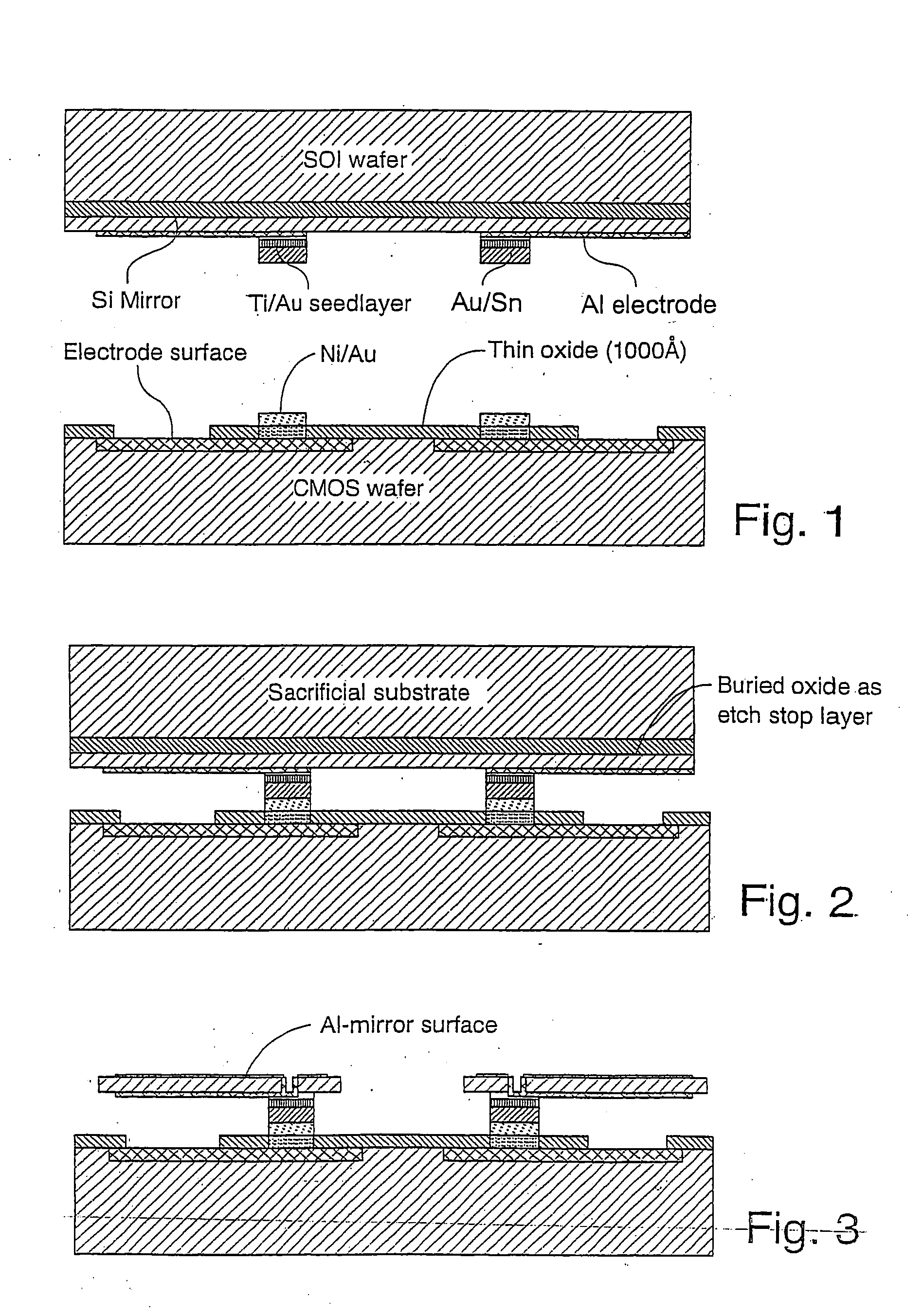
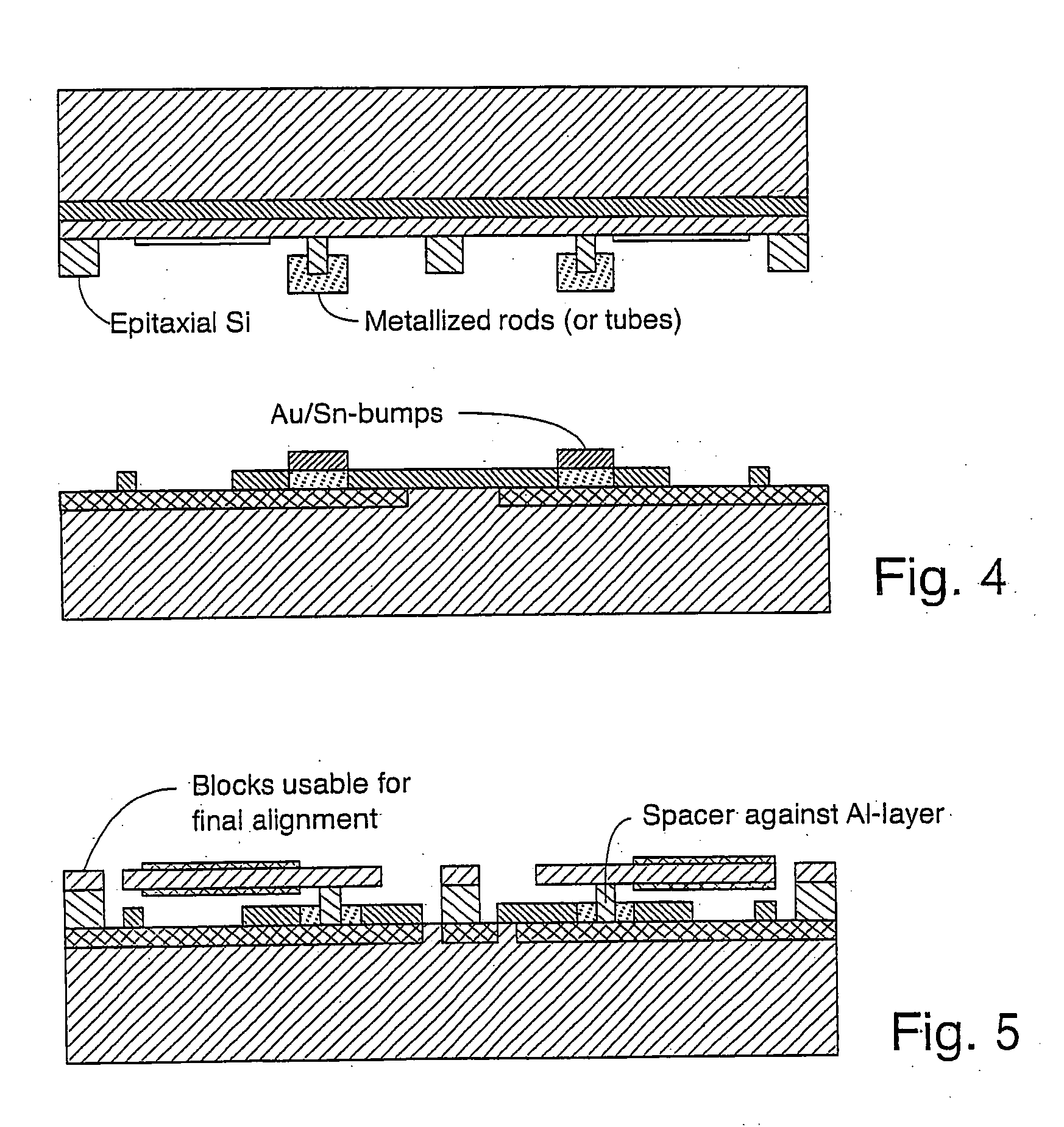
[0077] In summary the process can be described as follows with reference to FIGS. 6-7:
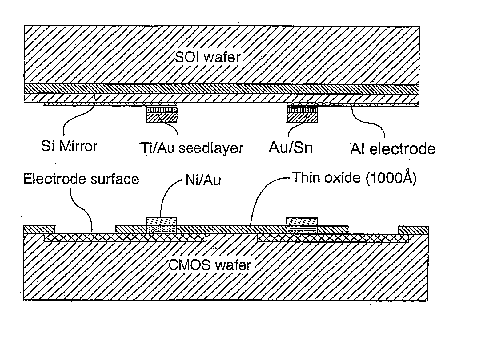
[0078] Making the SOI-wafer (Top-wafer) which is then normally is not processed further before the AuSi eutectic bonding. Optionally this wafer can be deposited with a metal layer as mirror electrodes following the processing according to embodiment 1.
[0079] The second wafer (bottom wafer in FIG. 6), which can be a CMOS wafer or a plain Si wafer structured or non-structured, comprises electrodes made by depositing suitable electrically conductive materials such as Al, Au, Ni, Ti etc or using highly doped silicon as it is or using a plain or structured wafer with wafer through vias (i.e. electrical connections through the wafer). The bottom wafer is also provided with eutectic bumps (as defined above) of e.g. Ni / Au or TiW / Au, consisting of a diffusion ba...
embodiment 4
[0084]FIG. 9 schematically shows a perspective view of a fourth embodiment of the final mirror or mirror arrays device fabricated according to the invention. For clarity the mirrors and hinge / suspension structures are removed in the right part of the drawing looking into the cavity where the electrodes are shown. FIG. 10 is a cross section at A-A′ in FIG. 9.
[0085] The process comprises making two separate wafers, a first wafer carrying the mono / single crystalline materials, e.g. silicon, GaAs, SiC etc, from which the mirror(s) are to be made, and a second wafer carrying components necessary for the function of the final mirror device such as electrodes, bond pads, via contacts, CMOS electronics. Then the two wafers are bonded together using an eutectic bonding method according to the present invention.
[0086] In summary the process can be described as follows:
[0087] Making the SOI-wafer (Top-wafer, FIG. 11): [0088] 1.—Evaporation or sputtering of thin layers of Ti / Au as electrode ...
embodiment 5
[0115] Similiar structure as embodiment 4 but placing the solder on top wafer and contact areas on the bottom wafer (as embodiment 1 but with the final structure according to embodiment 4).
PUM
 Abstract
Description
Claims
Application Information
 - R&D
- Intellectual Property
- Life Sciences
- Materials
- Tech Scout
- Unparalleled Data Quality
- Higher Quality Content
- 60% Fewer Hallucinations
Browse by: Latest US Patents, China's latest patents, Technical Efficacy Thesaurus, Application Domain, Technology Topic, Popular Technical Reports.
© 2025 PatSnap. All rights reserved.Legal|Privacy policy|Modern Slavery Act Transparency Statement|Sitemap|About US| Contact US: help@patsnap.com


