
Design method and implementation of optimal linear IIR equalizers for RF transceivers

Inactive Publication Date: 2005-05-12
AVAGO TECH WIRELESS IP SINGAPORE PTE
View PDF14 Cites 46 Cited by
  • Summary
  • Abstract
  • Description
  • Claims
  • Application Information

AI Technical Summary

Benefits of technology

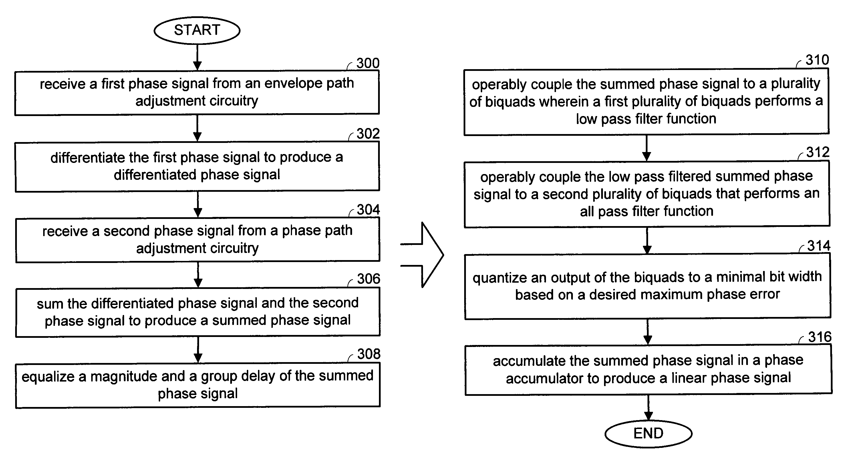
[0026] The apparatus and method of the present invention substantially solves these problems by implementing an architecture that employs a new digital processing sequence. Among other aspects of the inventive architecture, equalizers perform equalization prior to phase accumulation within phase accumulators. A phase differentiator receives an envelope path phase signal to produce a differentiated phase signal to the equalizer. The transfer function of the phase differentiator is implemented so that it cancels, except for a one cycle delay, the transfer function of the phase accumulator. This cancellation substantially eliminates accumulation of the envelope path phase signal.
[0027] To further improve effectiveness of circuitry that compensates for distortion in the transmit and receive paths of a transceiver, a method and corresponding circuitry is presented herein that facilitates generation of an optimal design for generating said compensation. The method for optimizing a linear equalizer of an RF transceiver generally includes selecting a desired filter response wherein the desired filter response matches a specified analog filter in a signal path, determining filter characteristics of the specified analog filter, generating a discrete time model of the specified analog filter based upon a desired signal filter response and upon the filter characteristics of the specified analog filter; determining a digital filter; determining total signal filtering of the RF transceiver based upon the discrete time model of the specified analog filter and upon characteristics of the digital filter; determining an inverse of the determined total signal filtering; multiplying the inverse of the determined total signal filtering with the determined total signal filtering to determine a desired equalizer filtering characteristic for pre-distorting group delay; optimally matching the desired equalizer filtering characteristic with an IIR magnitude equalizer to determine an optimal approximation of a magnitude response of the discrete time model of the specified analog filter; adding an inverse of the optimal approximation of the magnitude response to the desired equalizer filtering characteristic to determine pre-distorting group delay response of a filter; and optimally matching the pre-distorting group delay response of the filter to obtain an optimal approximation to the pre-distorting group delay response of the filter.

Problems solved by technology

In any mobile communication system the radio spectrum is a very limited resource shared by all users.
In practice, the power spectrum emitted from an EDGE transmitter will not be ideal due to various imperfections in the RF transmitter circuitry.
However, due to the variable envelope properties of the 8-PSK modulation option in EDGE, driving the PA in saturated mode is not possible.
Another potential cause of performance degradation of RF polar transmitters is the so-called reference feed-through caused by several phase locked loop component non-idealities, such as non-zero reset delay of the phase frequency detector (PFD) as well as mismatches between the “up” and “down” current sources of the charge pump.
Reference feed-through generates tones at the RF output offset by an amount equal to the reference frequency and may lead to violation of the spurious emissions requirements of the EDGE standard.
In practice, designing the PLL such that H(s)=1, i.e., has infinite bandwidth, is impossible.
Reference feed-through is the result of several PLL component non-idealities such as non-zero reset delay of the PFD, as well as mismatches between the “up” and “down” current sources of the charge pump.
For example, in GSM, where the RMS transmitter phase modulation error performance must be better than 5° and the peak modulation error must be better than 20°, designing the PLL filter narrower than 1 MHz leads to prohibitively large modulation errors.
In this case, the attenuation of reference feed-through by the PLL filter is limited and, for practical PFD reset delays and charge pump (CP) current source mismatches in a CMOS process, may not suffice to meet the spurious emissions requirements of the GSM standard as stated in the example.
Modulation error as a result of a narrow PLL signal filter is due to both amplitude distortion as well as group delay variation over the signal band of interest.
Stated differently, group delay variation causes different frequency components of the transmitter signal to travel through the transmitter at different speeds, thereby causing inter-symbol interference.
All of these effects add up to form the total modulation error.

Method used


Image

  • Design method and implementation of optimal linear IIR equalizers for RF transceivers
  • Design method and implementation of optimal linear IIR equalizers for RF transceivers
  • Design method and implementation of optimal linear IIR equalizers for RF transceivers

Examples


example 2

[0117] Consider a Butterworth type IF filter with a bandwidth of 800 kHz. The poles of such a filter are given in the following table and are specified in Radians / s:

p0−4900884.539 + j0p1−2450442.269 + j4244290.5123p2−2450442.269 + j4244290.5123

[0118] In this example, there is one real-valued pole and a pair of complex conjugate poles. Accordingly, the discrete-time equivalent filter corresponding to the impulse response invariance transformation with a sampling rate of 48 MHz is given by H⁡(z)=∑i=03⁢ ⁢ni⁢z-i∑i=03⁢ ⁢di⁢z-i(41)

[0119] where

n00.0andd0 1.0n10.00017172983538655d1−2.79466810430244n20.00065234568198411d2 2.60987701931729n30.00015495988000063d3−0.81422987961748

[0120] Suppose the desired receiver signal filter is a RRC with a roll-off factor of 0.4. FIG. 13 shows the magnitude responses of (1) square-root raised cosine filter with roll-off factor 0.4, (2) discrete-time model of the 800 kHz-bandwidth Butterworth filter, (3) digital channel select filter, and (4) desired o...

example 3

Discrete-Time Equivalent Model of the RF Transceiver Signal Filtering

[0123] In the following, a discrete-time model equivalent for the analog RF transceiver signal filter is derived. It is assumed that the signal filter can be represented as a rational function without repeated poles; that is, the Laplace transform of the signal filter can be written as H⁡(s)=∑i=0N-1⁢ ⁢bi⁢si∑i=0M-1⁢ ⁢ai⁢si=∑i=0M-1⁢ ⁢cis+pi(57)

where N1 are different.

[0124]FIG. 14 is a functional block diagram of a single-pole continuous-time system with zeroeth-order sample-and-hold function H1(s). To find the discrete-time equivalent filter with sampling period T, consider first the one-pole system depicted in FIG. 14. It will be shown that the discrete-time equivalent filter of this one-pole analog filter is given by: H⁡(z)≡Z⁢{y⁡(nT)}X⁡(z)=ab⁢(1-ⅇ-pT)⁢z-11-ⅇ-pT⁢z-1(45)

The principle of superposition that the discrete-time equivalent of the filter (19) is given by HDT⁡(z)=∑i=0M-1⁢ ⁢aibi⁢(1-ⅇ-pi⁢T)⁢z-11-ⅇ-pi⁢T⁢...


PUM


Abstract

A digital filter with equalizers and a corresponding method for optimizing a linear equalizer of an RF transceiver determining filter characteristics of the specified analog filter, determining total signal filtering of the RF transceiver based upon a discrete time model of the specified analog filter and upon characteristics of the digital filter, determining an inverse of the determined total signal filtering; multiplying the inverse of the determined total signal filtering with the determined total signal filtering and optimally matching the desired equalizer filtering characteristic with an IIR magnitude equalizer to determine an optimal approximation of a magnitude response of the discrete time model of the specified analog filter. Thereafter, the method includes adding an inverse of the optimal approximation of the magnitude response and optimally matching the pre-distorting group delay response of the filter to obtain an optimal approximation to the pre-distorting group delay response of the filter.

Description

CROSS REFERENCE TO RELATED PATENTS [0001] This application is a Continuation-in-Part of, claims priority to, and incorporates by reference the following U.S. Utility Applications under 35 U.S.C. 120: [0002] (1) “A Technique for Improving Modulation Performance of Translational Loop RF Transmitters (Attorney Docket No. BP 3019), having a Ser. No. 10 / 676,221 and a filing date of Sep. 30, 2003; [0003] (2) “A Digital Delay Element for Delay Mismatch Cancellation in Wireless Polar Transmitters” (Attorney Docket No. BP 3695), having a Ser. No. 10 / 925,485 and a filing date of Aug. 25, 2004; [0004] (3) “Architectural Techniques for Envelope and Phase Signal Alignment in RF Polar Transmitters Using Power Amplifier Feedback” (Attorney Docket No. BP 3796), having a Ser. No. 10 / 954,883 and a filing date of Sep. 30, 2004; [0005] (4) “Digital Algorithm for On-Line ACPR Optimization in Polar RF Transmitters” (Attorney Docket No. BP 3824), having a Ser. No. 10 / 944,551 and a filing date of Sep. 17, ...

Claims


Application Information

Patent Timeline
IPC IPC(8): H04L27/36
CPCH04L27/368
Inventor JENSEN, HENRIK T.
Owner AVAGO TECH WIRELESS IP SINGAPORE PTE
Learn More